
Pensieve Processing
- Assign: Tuesday, 2 October
- Checkpoint: Aim to complete 1-5 by 11:59pm on Friday, 5 October
- Due: Under the door of Ben's office (SCI S580) by 11:59pm on Thursday, 11 October
- Policy: Individual graded synthesis assignment
- Submit: A neat paper copy of the cs240-arch-worksheet.pdf submission sheet .
- Reference:
Note: You will be prepared for exercises #1-2 by partway through class on Friday 28 September. You will be prepared for all exercises except #6 by the end of class on Tuesday 2 October. We have extended the deadline to after Fall Break because we will cover material for #6 in class on Friday 5 October. Feel free to read ahead and complete that exercise before fall break. We recommend finishing most or all of the assignment before Fall Break, but you may turn it in as late as Thursday 11 October if you prefer. If you turn in the assignment before Fall Break or by the end of Wednesday 10 October, we should have it graded for you ahead of the exam that starts Friday 12 October.
Exercises
Please write your answers on the cs240-arch-worksheet.pdf submission sheet to streamline the grading process.
1. Flop-flip-flopping (7 points)
Consider the following circuit that uses falling-edge triggered D flip-flops.
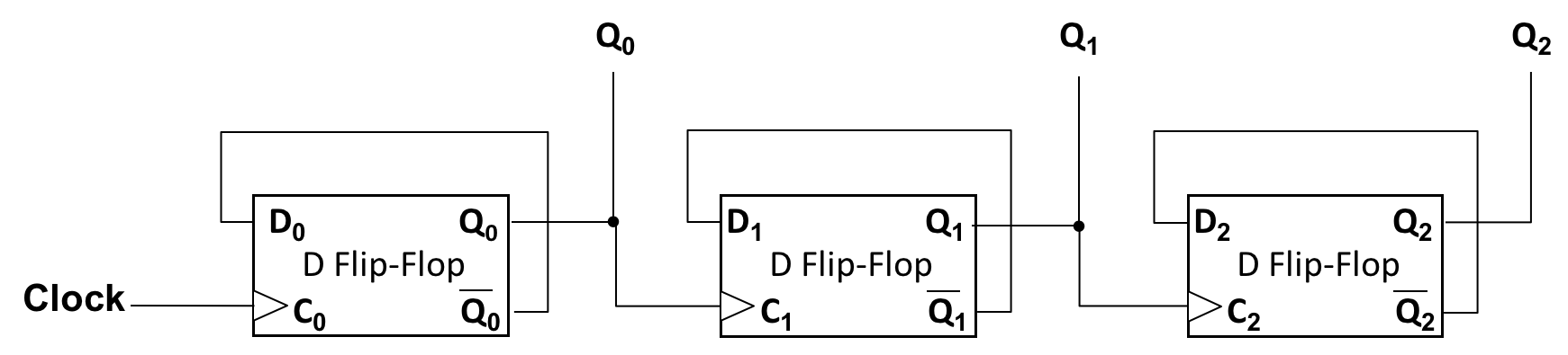
| Cycles Completed | Q2 | Q1 | Q0 |
| 0 (initial state) | 0 | 0 | 0 |
| 1 | |||
| 2 | |||
| … | |||
| 10 |
Assume the Clock input, and outputs Q0, Q1, and Q2, are all initially 0. Draw waveforms for Clock, Q0, Q1, and Q2, showing at least ten Clock cycles. You do not need to turn in your waveform drawing, but it will help you reason about the circuit.
-
Write a table summarizing the values of Q0, Q1, and Q2 after each Clock cycle.
-
Briefly explain what this circuit does at a high level, treating the Q outputs together. A phrase to a couple sentences is enough.
2. Reconstructing Memories (14 points)
In this set of exercises, you will reuse provided RAMs (random access memories) to design RAMs of different dimensions without reimplementing the internals.
Provided RAMs
In an A×B RAM, A is the number of addressable locations (cells) in the memory and B is the width of each location (cell) in bits. Recall that a RAM is much like a register file, but the underlying storage technology is not based on flip-flops. Memory addresses are analogous to register numbers in a register file; memory locations (cells) are analogous to registers in a register file. Unlike the register file we designed, these RAMs support reading only one location at a time.
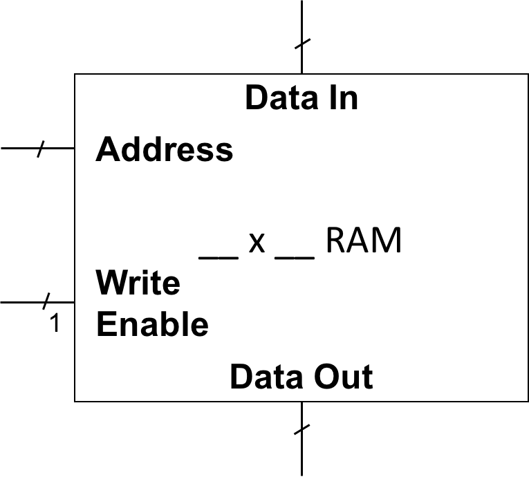
The provided RAMs have the following form:
- Each RAM has a Data In port, a Data Out port, an Address input and a Write Enable input.
- Each RAM is always reading from the location given by the current Address, expressing its contents on Data Out.
- Each RAM also stores the value on Data In into the location given by the current Address if the Write Enable input carries a 1.
- Each RAM is indivisible.
Rules
You will design new RAMs with the same kind of inputs, outputs, and externally observable behavior, but with different dimensions. For each:
- Draw one or more small boxes of the form above, representing the provided RAM(s), inside a larger box of the same form, representing the RAM you are implementing.
- Connect inputs and outputs of the larger box with those of the smaller boxes, possibly adding combinational logic building blocks.
- Do not draw each individual line of a bus (e.g., Address) unless necessary to distinguish the endpoints of the individual lines. Use hatch marks and width annotations instead.
Exercises
-
(4 points) Design a 256×8 RAM by adding minimal wiring and logic to two identical 256×4 RAM components. Label the widths (in bits/lines) of the ports Address, Data In, and Data Out for each 256×4 RAM you use and for the 256×4 RAM you implement.
-
(10 points) Design a 64K×8 RAM by adding minimal wiring and logic to a single provided 16K×32 RAM. (K = “kilo” = 1024)
- Unlike the previous exercise, this provided RAM component has
the same capacity as the desired final product, though it has
different dimensions:
- The provided RAM has fewer addressable memory locations (A) than the RAM you will design.
- The provided RAM has a larger addressable unit of data (B) than the RAM you will design.
- Be careful with writes: when writing an 8-bit value into the provided RAM, you must be sure to change only the relevant 8 bits of storage. All other storage bits should hold the same values as before the write operation.
- Unlike the previous exercise, this provided RAM component has
the same capacity as the desired final product, though it has
different dimensions:
3. Taking Control (7 points)
In this exercise you will design the Control Unit for the HW microarchitecture we designed in class. Our design focused on connecting the datapath components (e.g., the register file, ALU, memory, etc.), but we left the Control Unit as black box.
| Instruction | Opcode3:0 | Reg Write | ALU Op3:0 | Mem Store | Mem Load | Branch |
| LW | 0000 | |||||
| … | … | … | … | … | … | … |
Give a truth table with 4-bit HW instruction opcodes as inputs, plus one output for each of the control lines, outputs of the Control Unit that are control inputs to other components. The table should have one row for each of the seven instructions (one row for each opcode) except JMP from the first instruction table here.) The control lines we need are:
- Reg Write (1 bit): controls the write-enable of the register file.
- ALU Op (4 bits): controls the ALU (with the same 4 ALU control lines
we developed earlier).
- From left to right: Invert A, Negate B, Op1, Op0.
- Mem Store (1 bit): controls the write-enable of the data memory.
- Mem Load (1 bit): controls three multiplexers deciding which input
to provide for:
- the register file’s write address;
- the register file’s write data; and
- the ALU’s second operand.
- Branch (1 bit, added during class): controls whether to choose the next PC based on a branch target and test
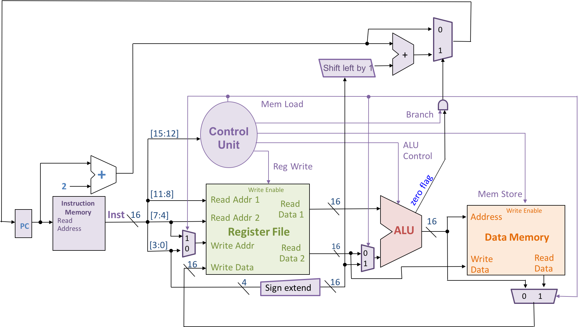
4. Jumping into the Unknown (14 points)
-
(8 points) Add logic to the HW microarchitecture to implement the
JMPinstruction, which we did not implement in class. You will add:- One new Jump control line from the Control Unit, carrying 1 if
the current instruction is
JMPand 0 otherwise. - One new column in the Control Unit table for the Jump control line.
- One new row in the Control Unit table for the
JMPopcode. - Wiring and logic using the Jump control line and the offset
bits from the
JMPinstruction encoding to store theJMPinstructions’s target address to the PC if and only if the current instruction isJMP. You will need to “cut” one existing wire to splice in some new logic.
JMPsets the PC to the absolute instruction address given by its argument (a number) multiplied by 2. For example,JMP 3sets the PC to 0x6, causing the instruction stored at address 0x6 (i.e., the 3rd instruction in the program) to be executed next. - One new Jump control line from the Control Unit, carrying 1 if
the current instruction is
-
(6 points) Assume
R2andR3hold input values when the following program starts.R4will hold an output when the program stops. The address of each instruction in the instruction memory is shown at left. The (new)HALTinstruction stops the computer.- Execute the program assuming
R2holds 5 andR3holds 2. What value doesR4hold when the computer reachesHALT? - Try a couple more examples with (small) positive numbers in
R2andR3. What does this code do withR2andR3to computeR4? Answer with one simple line of C code using variablesR2,R3, andR4with any operations (i.e.,R4 = ...;).
- Execute the program assuming
    # R2 and R3 hold program inputs here.
0:  AND R2, R2, R4
2:  AND R3, R3, R5
4:  BEQ R5, R0, 3
6:  SUB R5, R1, R5
8:  ADD R4, R4, R4
A:  JMP 2
C:  HALT # Stops execution.
    # What value is in R4?
5. Instruction Not Missing (12 points)
The HW ISA introduced in class lacks an instruction for bitwise
complement. A logical choice would be NOT Rs,Rd, which takes the
bitwise complement of the value in source register Rs and stores
into destination register Rd. You will design two implementations
of the proposed NOT instruction.
-
(4 points) One way to implement
NOTis to replace any occurence of aNOTinstruction by a sequence of existing HW instructions that has the same effect asNOT.Given source register identifier
Rsand destination register identifierRd, write a sequence of one or more HW instructions that has the same effect asNOT Rs,Rd. The replacement instructions may use values from any registers, but must store values only inRd. Instructions may not store values in any other register or data memory location. The sequence may use only the instructions defined in class. (See the instruction table here.)Hint: Think about the relation of bitwise complement and arithmetic rules.
-
(4 points) A second way to implement
NOTis to add a new instruction to the ISA, complete with an unique encoding, and to extend the microarchitecture to implement it. First, implement a related instruction (NAND) in this way.- Define a 16-bit encoding of the
NANDinstruction as in the instruction table here. Choose an unused opcode for the encoding. - Add a row to the Control Unit Table from Problem 3 to indicate
how to control the datapath to implement
NAND. Do not add extra logic to the datapath.
- Define a 16-bit encoding of the
-
(4 points) Consider how to implement
NOTusingNAND. Define an encoding for theNOTinstruction directly in the ISA. Choose the encoding carefully to minimize additions to the Control Unit and the datapath. Assuming you have completed (b), an ideal encoding requires no new rows or columns in the Control Unit table.Hint: Think of how to translate the
NOTinstruction to aNANDinstruction and use this intuition when designing the bit encoding ofNOT.
6. Points Affixed or Afloat in a C of Numbers (6 points)
-
[3 points] The Sea language (an imaginary programming language otherwise identical to C) supports a
signed fixed8ths chartype1 using an 8-bit signed fixed point number system with precision to the 1/8 (eighths) place.-
What are the minimum and maximum numbers representable by a
signed fixed8ths char? Write your answer as a base ten number using fractions or decimals. -
What are the minimum and maximum numbers representable by a
signed fixed32nds char, which uses 8-bit signed fixed-point representation with precision to the 32nds place? Write your answer as a base ten number using fractions or decimals. -

8-bit two's complement adder.
A, B, and Sum are 8-bit buses.We provide a hardware adder design (at right) that supports 8-bit two’s complement addition (e.g., for
signed charnumbers). Draw a logic diagram for a hardware adder that supports thesigned fixed8ths charnumber system. You may use the provided two’s complement adder as a black box (no need to draw the internals) and extend it with whatever wiring and logic is necessary. There is a “trick” here! Keep it simple.
-
-
[3 points] Using the 6-bit floating-point encoding defined in class, give decimal notation of the numbers represented by the following floating-point encodings.
110101100001011100000011010010111101
-
charis often used for characters in C, including with literal character values like'c', but it is just a number type. It is synonymous withsigned charin most implementations, just a signed 8-bit integer.unsigned charis an unsigned 8-bit integer. ↩