
🔬 Lab
CS 240 Lab 3
Data as Bits
CS 240 Lab 3
Arithmetic Circuits
All the circuits you will work with today in lab are combinational circuits. Like basic gates, the output of combinational circuits depends only on the current inputs to the circuit. Combinational circuits are made with basic gates, but produce more complex functions.
Certain functions are very useful for a variety of tasks that help us design important components of a computer, so we examine them here. These include the multiplexer, decoder, demultiplexer, encoder, and the adder (the basic arithmetic circuit for addition).
Multiplexer
Exercise 1:
Although you may not have realized it, in the first problem on the lab assignment, you designed a simple 2x1 multiplexer (MUX), which you have also learned about in lecture.
A multiplexer can be thought of as a steering circuit, which steers a single input from a set of inputs through to the output, based on the select line.
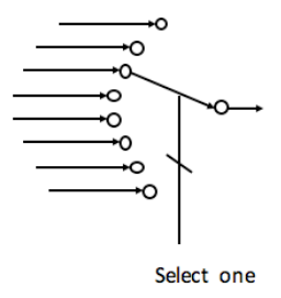
A schematic diagram showing conceptually how an 8x1 mux works.

The logic diagram symbol for a 2x1 mux.
Here’s a simulated version of a 4x1 mux (note how to select among 4 data inputs, 2 select inputs are needed):
Edit the circuit above by removing components to create a 2x1 mux, or if you prefer, build a 2x1 mux in LogicWorks. Verify that it works by manipulating your inputs and observing the output, and then describe your circuit below:
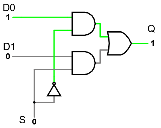
Inputs D0 and D1 each connect to a separate AND gate. The other inputs of those and gates connect to the S selector input, but with a NOT gate on the way for the AND gate connected to input D0. This means that switching S back and forth switches which AND gate gets activated by the S input, but only one of them does at a time. Both AND gates connect to an OR gate whose output is the circuit output.
How many different input combinations should you test to thoroughly test the circuit? Correct answer: 8
Exercise 2:
An 8x1 MUX (device shown on right below) has 8 input lines D7 - D0, 3 select lines S2 – S0, and 1 output line Q (the device labeled DEV1 below is a LogicWorks 8x1 MUX).

Important: The EN input is an “enable” line – you must activate it for the device to work correctly. However, notice the small circle representing NOT attached to the EN input: this means that you should connect it to ground to activate it, rather than connecting it to +5V. These kinds of inverted connections are also called active low, since they’re active when the voltage is low, rather than when it’s high.
Use the Falstad window below, or create a new circuit in LogicWorks. Follow these steps:
LogicWorks
- Add an 8x1 mux (search for “Mux-8”).
- Connect the enable line to ground.
- Add a “Hex Keyboard w/o STB” and connect the three bottom pins to the S0, S1, and S2 inputs. Leave the top pin disconnected.
- Connect 8 binary switches as inputs D7-D0.
- Connect a binary probe to the output Q.
Falstad
- Add an 8x1 mux (“Draw -> Digital Chips -> Multiplexer”) to the circuit, above what’s already there. Edit the mux to increase the select lines from 2 to 3.
- Connect the select lines to the vertical wires coming up from the provided components. These components let you select a hex value: on the right under “Current Circuit” there is a “Voltage” slider. Drag it back and forth to manipulate the hex digit shown on the 7-segment LED display. Note that only 3 of the 4 bits are needed.
- Connect 8 logic inputs to the I0-I7 inputs. (Create one, swap it to numeric, then copy-paste).
- Connect a logic output to the output Q.
Click on the hex keyboard (LogicWorks) or drag the slider (Falstad) to change the select lines.
At this point, demonstrate to the instructor that you understand how the multiplexer works.
Exercise 3:
A multiplexer can be used to implement any boolean function by hard-wiring the data inputs to fixed high or low values to correspond to the desired output for the function for given input combinations of the select lines.
This following truth table for a function Q indicates whether or not a 3-bit value S2 S1 S0 is a power of two:
| S2 | S1 | S0 | Q |
|---|---|---|---|
| 0 | 0 | 0 | 0 |
| 0 | 0 | 1 | 1 |
| 0 | 1 | 0 | 1 |
| 0 | 1 | 1 | 0 |
| 1 | 0 | 0 | 1 |
| 1 | 0 | 1 | 0 |
| 1 | 1 | 0 | 0 |
| 1 | 1 | 1 | 0 |
Here is a pin-out for a 74151 8x1 multiplexer:
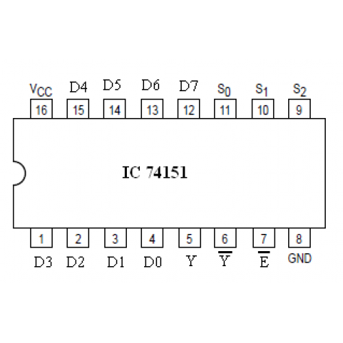
On your protoboard, there is a 74151 chip (8 x 1 MUX) inserted in the top-right area. Connect it to produce the function Q.
Output is measured at Y (pin 5). It is not necessary to use or connect pin 6.
Don’t forget the power(pin 16), ground (pin 8), and enable line (pin 7, connect to ground)!
Confused? Click here for hints.
The key to this exercise is to figure out what “hard-wiring the data inputs” means. The data inputs are D0-D7 (or in Falstad, I0-I7). Rather than connect these to switches, like you did in the previous exercise in the simulator, you’re going to connect each one directly to either +5V or ground, to establish a permanent high or low voltage signal for that input.
The goal given that info is to figure out: which data inputs should I connect to +5V and which should I connect to ground, in order to make the chip behave according to the specified truth table?
You will connect S0/S1/S2 to three of the logic switches, because those inputs are what you’ll be manipulating.
Demonstrate to the instructor that your circuit detects inputs on the select lines which represent a power of 2.
Decoder
Exercise 4:
A decoder has inputs and outputs. Only one of the outputs is active for any given -bit input combination.
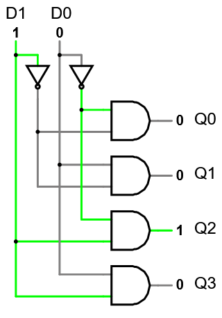
In the second problem on the pre-lab assignment, you designed a simple 2x4 decoder. Assuming 2 inputs A0 and A1 and 4 outputs D0 - D3, and:
D0 is only true when A1A0 = 00 D1 is only true when A1A0 = 01 D2 is only true when A1A0 = 10 D3 is only true when A1A0 = 11
This can be described by the following truth table:
| A1 | A0 | D0 | D1 | D2 | D3 |
|---|---|---|---|---|---|
| 0 | 0 | 1 | 0 | 0 | 0 |
| 0 | 1 | 0 | 1 | 0 | 0 |
| 1 | 0 | 0 | 0 | 1 | 0 |
| 1 | 1 | 0 | 0 | 0 | 1 |
Such a device is said to decode the binary number which is specified by the inputs, activating the output which corresponds to the decimal value of the binary input.
You should have designed a circuit that looks something like this:
Build the circuit for the 2x4 decoder in LogicWorks or the Falstad simulator (blank window below) using basic gates.
Demonstrate correct operation to the instructor.
Exercise 5:
The 74138 is a 3x8 decoder chip. You will find one inserted in the bottom-right corner of your protoboard. Below is a pin-out for the 74138:
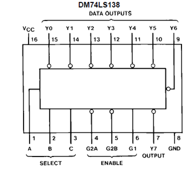
Make the following connections to the device:
- Connect VCC pin to voltage and GND pin to ground on the board.
- Connect the SELECT lines A B C on the chip to 3 Logic Switches on the board.
- Connect each of the 8 DATA OUTPUTS on the chip to Logic Indicators on the board.
- Connect the ENABLE lines G2A and G2B to ground on the board.
- Connect the ENABLE line G1 to voltage on the board.
Now complete this truth table based on your observations of the decoder:
GCorrect answer:
| C | B | A | Y0 | Y1 | Y2 | Y3 | Y4 | Y5 | Y6 | Y7 |
|---|---|---|---|---|---|---|---|---|---|---|
| 0 | 0 | 0 | 0 1 |
0 1 |
0 1 |
0 1 |
0 1 |
0 1 |
0 1 |
0 1 |
| 0 | 0 | 1 | 0 1 |
0 1 |
0 1 |
0 1 |
0 1 |
0 1 |
0 1 |
0 1 |
| 0 | 1 | 0 | 0 1 |
0 1 |
0 1 |
0 1 |
0 1 |
0 1 |
0 1 |
0 1 |
| 0 | 1 | 1 | 0 1 |
0 1 |
0 1 |
0 1 |
0 1 |
0 1 |
0 1 |
0 1 |
| 1 | 0 | 0 | 0 1 |
0 1 |
0 1 |
0 1 |
0 1 |
0 1 |
0 1 |
0 1 |
| 1 | 0 | 1 | 0 1 |
0 1 |
0 1 |
0 1 |
0 1 |
0 1 |
0 1 |
0 1 |
| 1 | 1 | 0 | 0 1 |
0 1 |
0 1 |
0 1 |
0 1 |
0 1 |
0 1 |
0 1 |
| 1 | 1 | 1 | 0 1 |
0 1 |
0 1 |
0 1 |
0 1 |
0 1 |
0 1 |
0 1 |
Check AnswersCorrect answer: See above
The outputs for this device are active low. Describe what that means in your own words:
Example answer: It means that instead of high-voltage meaning ‘active’ while low voltage means ‘inactive,’ the opposite is true: low-voltage means ‘active’ and high-voltage means ‘inactive.’
Demultiplexer
A demultiplexer is the exact opposite of the multiplexer.

The demultiplexer takes one single input data line and then switches it to only one of the individual output lines at a time based on selector inputs, leaving the rest of the output lines low.
Exercise 6:
Complete the truth table for the 1x4 demultiplexer with select lines S1 and S0 and input D.
GCorrect answer:
| S1 | S0 | D | Q3 | Q2 | Q1 | Q0 |
|---|---|---|---|---|---|---|
| 0 | 0 | 0 | 0 1 |
0 1 |
0 1 |
0 1 |
| 0 | 0 | 1 | 0 1 |
0 1 |
0 1 |
0 1 |
| 0 | 1 | 0 | 0 1 |
0 1 |
0 1 |
0 1 |
| 0 | 1 | 1 | 0 1 |
0 1 |
0 1 |
0 1 |
| 1 | 0 | 0 | 0 1 |
0 1 |
0 1 |
0 1 |
| 1 | 0 | 1 | 0 1 |
0 1 |
0 1 |
0 1 |
| 1 | 1 | 0 | 0 1 |
0 1 |
0 1 |
0 1 |
| 1 | 1 | 1 | 0 1 |
0 1 |
0 1 |
0 1 |
Check AnswersCorrect answer: See above
Why are there some rows in the table where all of the data outputs are zeroes?
Example answer: Because if the input is 0, it doesn’t matter where it gets directed to, that line will be a 0 and the others will be zeroes by default.
Complete the Boolean algebra function for each output:
Q3 = Example answer: S1S0D
Q2 = Example answer: S1S0’D
Q1 = Example answer: S1’S0D
Q0 = Example answer: S1’S0’D
Encoder
An encoder is the exact opposite of the decoder.

It takes inputs (it is assumed that only 1 of the inputs can be active at a time). The input number of the input that’s active specifies a decimal number, which gets translated to binary on the output lines.
Exercise 7:
Complete the truth table for the 4x2 encoder:
GCorrect answer:
| D3 | D2 | D1 | D0 | Q1 | Q0 |
|---|---|---|---|---|---|
| 0 | 0 | 0 | 1 | 0 1 |
0 1 |
| 0 | 0 | 1 | 0 | 0 1 |
0 1 |
| 0 | 1 | 0 | 0 | 0 1 |
0 1 |
| 1 | 0 | 0 | 0 | 0 1 |
0 1 |
Check AnswersCorrect answer: See above
Complete the Boolean algebra function for each output:
Q1 = Example answer: D3 + D2
Q0 = Example answer: D1 + D3
Why doesn’t D0 appear in either equation above?
Example
answer: Because when D0 is the input that’s
on, the correct output is 00, and so neither output
variable is true. Boolean algebra formulas express what’s necessary to
make something true, and they are false under any other
condition.
Stretch Material: Addition
In the pre-lab assignment for today, you saw that you can represent the sum of two single bit numbers A and B with the following truth table:
| A | B | CarryOut | Sum |
|---|---|---|---|
| 0 | 0 | 0 | 0 |
| 0 | 1 | 0 | 1 |
| 1 | 0 | 0 | 1 |
| 1 | 1 | 1 | 0 |
This points to the following logical formulae:
CarryOut = A AND B
Sum = A XOR B
Exercise 8:
Using LogicWorks or the Falstad simulator, build the circuit which produces Sum and CarryOut from inputs A and B (this circuit is known as a half adder). You should use exactly one AND gate and one XOR gate.
Demonstrate to the instructor that your circuit works correctly.
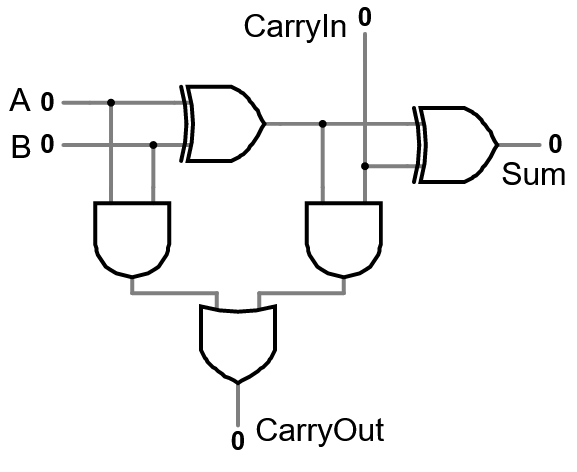
The following is the truth table for a full adder (which incorporates a carry-in bit to the sum of A and B):
| CarryIn | A | B | CarryOut | Sum |
|---|---|---|---|---|
| 0 | 0 | 0 | 0 | 0 |
| 0 | 0 | 1 | 0 | 1 |
| 0 | 1 | 0 | 0 | 1 |
| 0 | 1 | 1 | 1 | 0 |
| 1 | 0 | 0 | 0 | 1 |
| 1 | 0 | 1 | 1 | 0 |
| 1 | 1 | 0 | 1 | 0 |
| 1 | 1 | 1 | 1 | 1 |
The circuit for the full adder is:
Exercise 9:
Revise your circuit from the previous exercise to build a full adder.
Demonstrate its operation to the instructor.
Stretch Material: IC 7483
You will find an IC 7483 inserted in the middle section of your protoboard. Here is a logic diagram of the chip (as usual, actual pins are numbered counterclockwise around the chip from 1 at the top left), along with a diagram showing the ordering for the input connections:
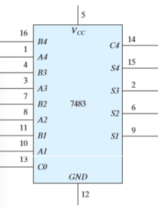
Logic diagram (NOT a pinout) for the 7483.
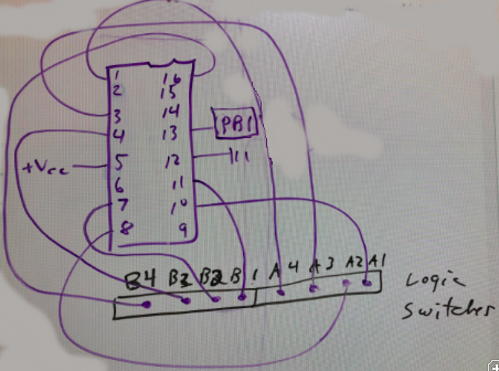
How to connect the inputs (output connections not shown). Ordering and grouping of A and B inputs is important.
Exercise 10:
Wire up the chip, following these guidelines:
- Use logic switches on the board for the A and B inputs, and the PB1 switch for C0.
- It is best to group the A switches next to one another (don’t alternate with the B switches), and arrange the input switches so the most significant bit is on the left (see diagram on the right).
- Connect all 5 outputs to logic indicators, in order with S1 on the right, S2 to its left, etc. Leave a gap between S4 and C4 for clarity.
- Don’t forget to connect Vcc and GND.
REMEMBER: the actual chip layout has pin 1 on the upper left, with 8 pins on each side of the chip numbered counterclockwise around it.
Now that it’s working, perform the following tests:
Set the A4 A3 A2 A1 and B4 B3 B2 B1 inputs to the numbers shown below, and record the outputs for each setting:
A inputs 0001
B inputs 0001
C0 off (i.e., 0)
GCorrect answer:
C4 0
1
S4 0
1
S3 0
1
S2 0
1
S1 0
1
Check AnswersCorrect answer: See above
A inputs 0010
B inputs 0011
C0 off (i.e., 0)
GCorrect answer:
C4 0
1
S4 0
1
S3 0
1
S2 0
1
S1 0
1
Check AnswersCorrect answer: See above
A inputs 0010
B inputs 0011
C0 pressed (i.e., 1)
GCorrect answer:
C4 0
1
S4 0
1
S3 0
1
S2 0
1
S1 0
1
Check AnswersCorrect answer: See above
What function do you think the chip is performing?
Example answer: 4-bit addition, with carry-in and carry-out.
What is the purpose of C4? Is it correct for the calculations above?
Example answer: C4 is the carry-out bit. It’s off in all results above, as it should be.
Next, set A to 1010 and B to 1111 leaving C0 off, and record the result:
GCorrect answer:
C4 0
1
S4 0
1
S3 0
1
S2 0
1
S1 0
1
Check AnswersCorrect answer: See above
Click to select answers for these questions, assuming a 4-bit two’s-complement (i.e., signed) representation:
GCorrect answer:
Is this result correct? no
yes
Is there carry-out? no
yes
Is there overflow? no
yes
Check AnswersCorrect answer: See above
Extra Exercises: 4-bit Ripple-Carry Adder
It turns out that once you have a 1-bit adder, you can do -bit addition by using 1-bit adders: one for each matched pair of bits in the two -bit numbers being added. The CarryOut for each pair of bits becomes the CarryIn for the next most significant pair of bits in the numbers. This is known as a ripple-carry adder.
Exercise 10:
Use either LogicWorks or the Falstad simulator to build a 4-bit adder out of 1-bit adders:
LogicWorks
- Download this 4bit-adder circuit template and then open it in LogicWorks. It contains four 1-bit adders (the adder device is an abstraction for the 1-bit full adder you experimented with earlier).
- Add hex keyboards for the A and B inputs. Connect the individual bits from each keyboard to one of the 1-bit adders.
- Add a “Hex Display” and connect the four outputs to it.
- Add a binary switch for the carry-in and a binary probe for the carry-out.
- Connect the carry-out / carry-in lines between each of the adders.
Falstad
- Start from the circuit below, which includes 4 1-bit adders, 8 logic inputs, and hex displays for both the two inputs and the output.
- You do NOT need to connect anything to the bottom displays, they will display the inputs automatically once everything is hooked up.
- Connect the 8 inputs to the 8 input lines of the 4 adders. Make sure to connect A0/B0 to the bottom adder and move upwards from there.
- Add a 9th input for the carry-in.
- Add a logic output for the carry-out.
- Connect together the carry-out / carry-in lines between the adders.
- Connect the S outputs to the I0-I3 inputs to the display at the top right.
Perform the following tests to verify the circuit:
2 + 5 = Correct answer: 7
A + 3 = Correct answer: D
A + A = Correct answer: 4 (should have carry-out; this is overflow)
6 + 5 = Correct answer: B (no carry-out, but this is overflow)
F + F (with carry-in on) = Correct answer: F (carry-out and overflow)
Extra Practice
Exercise 11:
Build a 1x4 demultiplexer and/or a 4x2 encoder in LogicWorks or the Falstad simulator (blank window below):
Exercise 12:
Hook up two 4-bit adders to create an 8-bit adder. Note: In Falstad, you can right-click an adder to select how many bits you want.