CS 240 Lab 4: ALU and Sequential Logic
Peter Mawhorter
How do Computers Work?
How do Computer Circuits Work?
- Power flows through chips in the computer, creating patterns of
activation driven by a clock and determined by logic gates.
- Inputs like a keyboard feed into these patterns.
- Some of these patterns drive outputs like a monitor.
How do Computers Represent Things?
- High/low voltage patterns represent numbers in binary and/or symbols.
- The computer performs basic operations with these numbers, like
addition, through the use of specialized chips.
- All other operations are built from a series of basic operations.
But what about… ?
- Integrated circuits put together gates to perform various functions. Which circuits are used in a CPU, and what are their functions?
- How do the integrated circuits for basic binary operations like addition work?
- How are clock signals generated & managed in the computer?
- How is memory implemented using gates?
- How can we change what a computer does by writing a program, instead of having to re-wire it?
How does the OS Work?
- When you boot the computer, it launches an operating
system, which provides control interfaces.
- Usually there is graphical output and keyboard or touch input.
- Servers are controlled remotely via text (a shell/terminal/command line).
- OS allows user to launch programs, including custom programs.
- Programs are files on the computer.
But what about… ?
- How does the “boot” process work? Where does the operating system actually start?
- What language does the “shell” use? Why are shells still around when we have graphical interfaces?
- How does one program launch another? How does the OS keep track of programs that are running? How do two programs run at the same time?
- How do compliers actually work? How does our text written in a programming language turn into a program, and what does a “program” actually consist of?
What we’ll see today
- How do the integrated circuits for basic binary operations like addition work?
- How are clock signals generated & managed in the computer?
- How is memory implemented using gates?
Outline
Arithmetic Logic Unit
Arithmetic Logic Unit
- A multi-function circuit that operates on binary values A and B producing a result R.
- 2-bit Op1/Op0 inputs select the
operation: AND, OR, or +
- NOR and - can be achieved using invertA and negateB
- invertA just inverts each bit of A
- negateB inverts each bit of B, and also sets the CarryIn bit
Arithmetic Logic Unit
- Has CarryOut, Sign,
Overflow, and Zero outputs in addition
to the output bits R
- CarryOut is the carry-out from addition (still present when a different operation is selected)
- Sign is just the highest bit of R
- Overflow is true when there’s two’s-complement overflow
- Zero is true when all of the R bits are zero
Arithmetic Logic Unit
| invA | negB | Op1 | Op0 | R |
|---|---|---|---|---|
| 0 | 0 | 0 | 0 | A AND B |
| 0 | 0 | 0 | 1 | A OR B |
| 0 | 0 | 1 | 0 | A + B |
| 0 | 1 | 1 | 0 | A - B |
| 1 | 1 | 0 | 0 | A NOR B |
(other combinations are possible)
Arithmetic Logic Unit
The ALU is the heart of the computer: everything a computer does is a transformation of data, and the ALU is what performs those transformations.
Memory
Memory
- Need to store + retrieve values for the ALU to work on
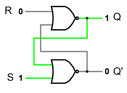
- An SR latch can be “set” or “reset”
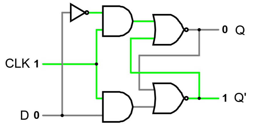
- A D latch stores one bit of “data”
- A D flip-flop reads only on the clock edge
Bistable Circuits
- Until now, we solved for voltage
- A bistable circuit has two different voltage
patterns that are equally stable.
- Must use assumptions to solve for voltage
- Look for two different solutions
SR Latch
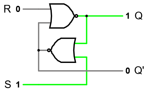
- S sets the latch (Q=1)
- R resets the latch (Q=0)
- Q and Q’ should be opposites
- Both are off when S=R=1
- When S=R=0, it remembers
- Race condition going from S=R=1to S=R=0
SR Latch Alternates
Clocks
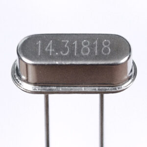
- Need to synchronize circuit changes
- Want some parts to activate only when selected
- A “clock” input can be either of these
- Has to change from +5V to 0V quickly
- Needs to be distributed to all parts of the processor
- Can use ~30% of the power in a CPU
Clock Signals
- In each cycle the clock is on for a time and then off for a time
- When the signal changes, that’s a rising or falling edge
- The period is the time between rising edges
- The frequency of the clock is 1/period
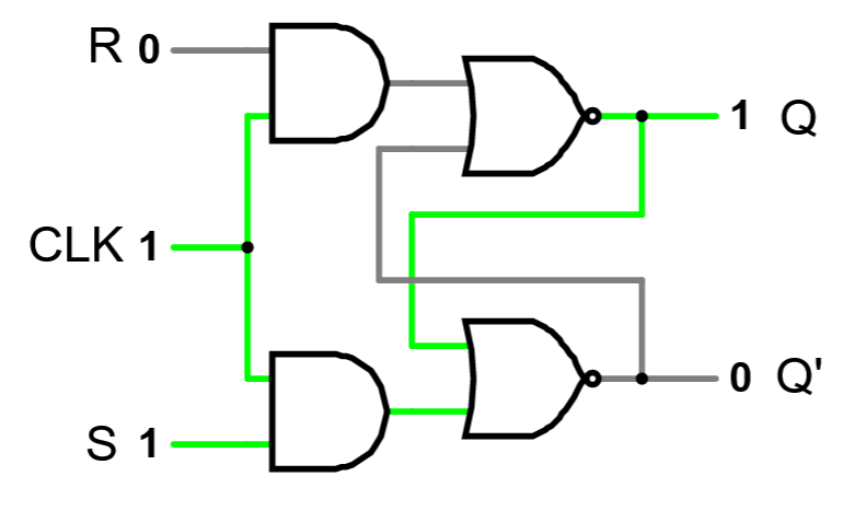
Clocked SR Latch
- When clock is off, latch remembers
- When clock is on, set and/or reset inputs can go in
- “Clock” may really be “write”
- Now if S=R=1 and we turn the clock off, we easily trigger the race condition
D Latch
- When D is high, we have S=1 / R=0
- When D is low, we have S=0 / R=1
- S=R=1 is impossible
- S=R=0 only when clock/write is low
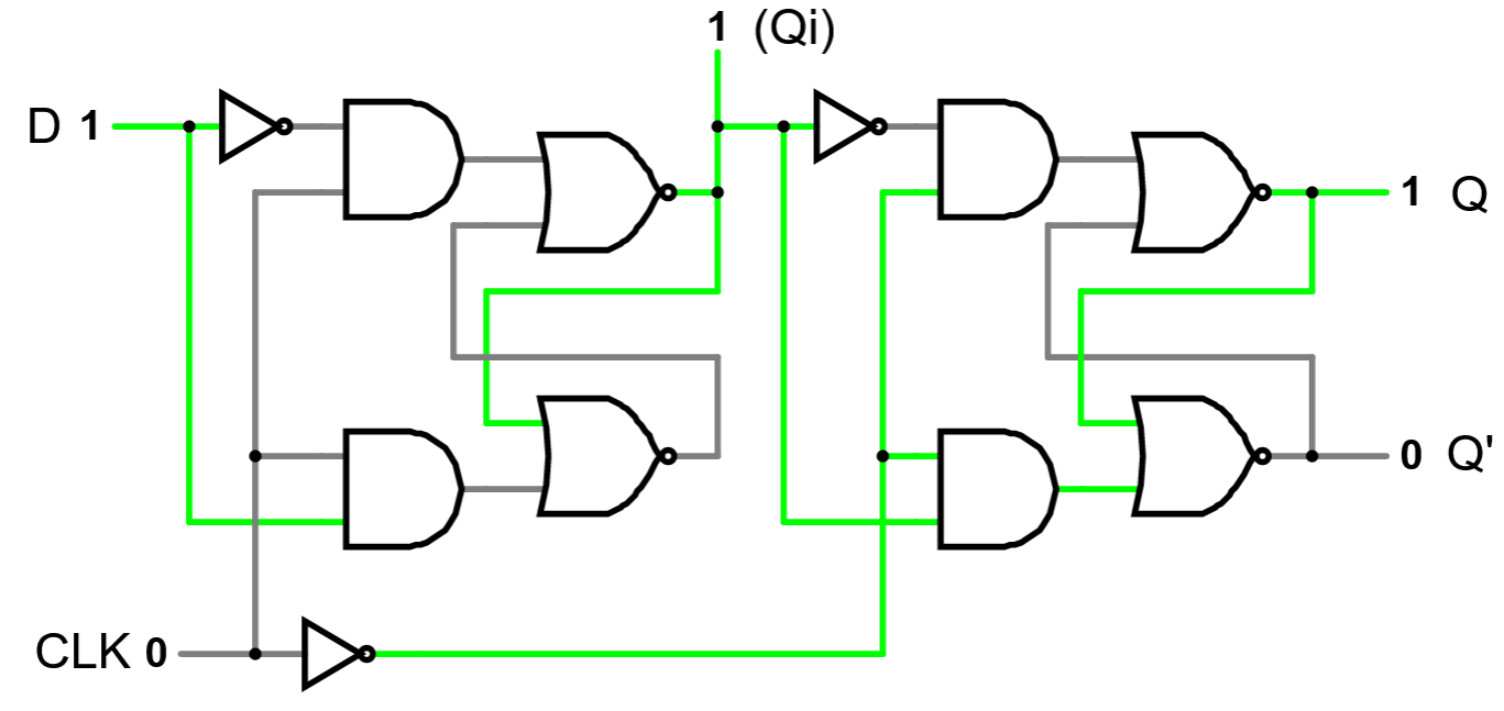
D Flip-Flop
- Captures state of D at falling clock edge
- Broadcasts old D value during entire clock ON pulse
Flip-Flop Timing
- Clock goes ON (rising edge)
- ALU etc. start their work to get results
- Have until the end of the clock pulse to settle
- Flip-flops still broadcast previous-cycle results
- Clock goes OFF (falling edge)
- Flip-flops capture new results
- Stuff can settle down until next rising edge
Remember that “clock” could be “write data pulse.”
Memory Organization
Register Files
- Multiple D flip-flops make up a register
- Common clock input; different data inputs/outputs
- A register file has multiple registers
- Multiplexers & decoders select register(s) to write/read
- Often has 2 output blocks & one input block since ALU needs 2 inputs and has 1 output each cycle.
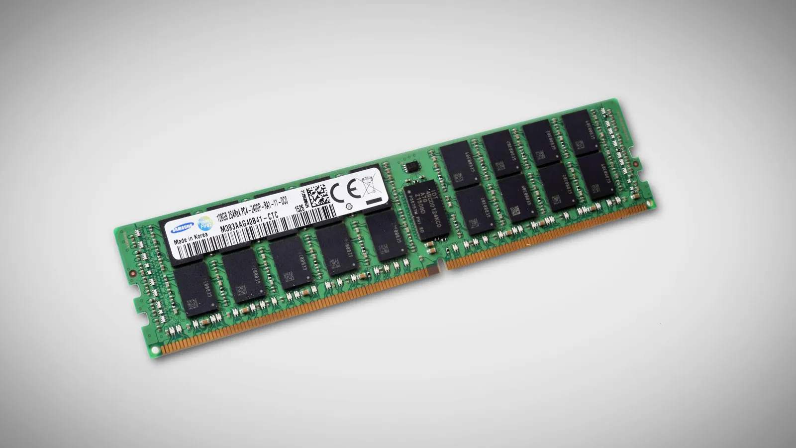
RAM
- Random Access Memory or RAM stores
lots of data
- Organized into n-bit words of data
- Each word has an address
- Same mechanisms as a register file
- Different tech (bigger/slower/cheaper)
