CS 240 Lab 2: Data as Bits
Peter Mawhorter
How do Computers Work?
When you press the power button, electricity flows through a bunch of transistors. This feeds power to things like a keyboard & monitor, which send inputs into or receive outputs from the transistors.
The transistors are organized into logic gates, like AND and OR.
But what about… ?
- There are tens of billions of transistors in a modern computer. How are they connected?
- Transistors have 1 input & 1 output. How do we represent numbers or text?
- Logic gates just compute a single outcome from some inputs. How do computers deal with signals over time? How is memory implemented?
- How can we change what a computer does by writing a program, instead of having to re-wire it?
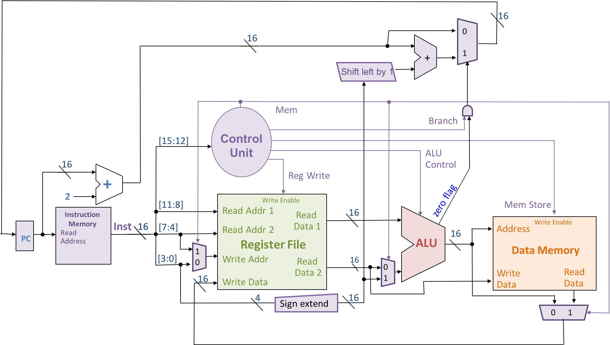
The schematic diagram of the full CPU.
The CPU connections listed as a table:
| Component | Inputs | Outputs |
|---|---|---|
| PC |
|
|
| Instruction Memory |
|
|
| Control Unit |
|
|
| Register File |
|
|
| Arithmetic Logic Unit (ALU) |
|
|
| Data Memory (RAM) |
|
|
| BEQ Logic |
|
|
Outline
Setup status?
- Has everyone successfully configured your CS account for CS 240?
- (First two sections of task 1 for the Zero assignment).
- Questions about
cs240script orgit?
Representing Numbers
Representing Numbers
- Binary represents numbers using 0 and 1
- In base 10, each digit represents
- 1, 10, 100, 1000, etc.
- In base 2 (binary), each digit represents
- 1, 2, 4, 8, 16, 32, 64, 256, 512, 1024, etc.
- We call these digits “bits”
- These numbers show up everywhere in CS
- In base 10, each digit represents
- We use a suffix when base is unclear:
- For example,
Converting to Binary
- Figure out biggest power-of-2 that’s smaller
- Hint: 1024 is
- This is the largest bit that’s a 1
- Repeat with the remainder after subtraction
Hexadecimal
- Binary numbers are long and hard to read
- Decimal numbers are hard to convert to/from binary
- Hexadecimal is a compromise: base-16
- Because the base is a power-of-2, conversion to/from binary is easy
- Large enough to be short
- Close enough to base-10 to be somewhat intuitive
Hexadecimal
- Uses letters A-F in addition to numbers 0-9
- Each digit is , and converts to/from 4 bits
- A
0xprefix is often used, e.g.,0xF83A - Two hex digits are 8 bits, which is a byte
- Bytes are a common unit of information because one byte is enough to represent any letter of the Latin alphabet + plenty of symbols (see ASCII)
- Max value of a byte is 255, which is
FFin hex
- Converting to binary: convert each digit + concatenate
Two’s Complement
How to represent negative numbers using bits?
- Could use one bit to represent +/-, and leave other bits alone
- 4 bits would represent -7 () to +7 (), including +0 () and -0 ()
- Adding two negative numbers requires special logic
- Instead, let the first bit represent
and then other bits add to that to bring us closer to 0.
- Now 4 bits can represent -8 () to +7 (), with just one 0 (). -1 is represented as -8 + 7 = .
Advantages of Two’s Complement
- Only one zero (simplifies equality checking)
- Addition & subtraction work using a single algorithm for
positive and negative numbers
- When adding a positive number to a negative number, the overflow into the sign bit will correctly determine whether the result is positive or negative
- See this StackOverflow answer for more.
Simulating Circuits
Simulating Circuits
- Two different simulators: CircuitVerse, and the Falstad simulator.
- CircuitVerse has more functionality for complex logic circuits,
while the Falstad simulator is easier to embed in notebooks.
- We’ll be designing circuits using CircuitVerse but will see the Falstad simulator in some slides & notebooks for examples.
CircuitVerse
- Cursor
- Click to select
- Drag green circles to draw wires
- Delete key to remove
- “Circuit Elements” panel click to add things.
- Timing window.
- Use “Debug flag” from “Misc” group.
- Properties panel (add labels, set bit width)
Wires may be “buses:” check ‘bit width’ of components
- Use “Splitter” under “Misc” group (a.k.a. breakout)
- Type total bits at first prompt and then group sizes at second prompt
- ‘8’ and then ‘2 3 3’ → break out 8 wires into 3 groups: 2 then 3 then 3
- ‘4’ and then ‘1 1 1 1’ → break a 4-wire bus into 4 individual wires
CircuitVerse Components
- “Input” includes power, ground, and editable inputs
- “Output” includes LEDs and hex displays plus output bits
- “Misc” has debug flag, splitter, and adder
- Other groups are useful too
- “Help” in the “Properties” panel has details
CircuitVerse Issues
- Sometimes “Preview Circuit” is more stable.
- Blue loading square: Select “save online” and then hit cancel.
- Sometimes gets stuck loading in Firefox. Workaround:
- Open dev tools under the three-bars-menu -> “More tools” -> “Web Developer Tools”
- Use arrows/more button near top where it says “Inspector” to open “Performance”
- Click “Start recording” and it should load
- Click “Cancel recording” and close dev tools
Counting with a Circuit
Logic Diagrams
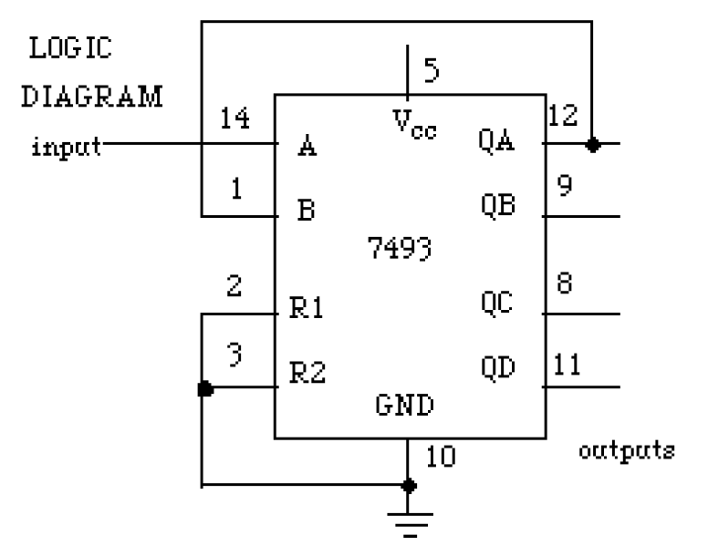
- NOT the same as a pinout.
- Inputs on the left
- Outputs on the right
- Voltage on top
- Ground on bottom
Logic Diagrams
- The layout inside a chip is set up to minimize fabrication costs, not to make your life easy.
- When wiring things on the protoboard, ignore the logic diagram layout and just pay attention to the pin numbers.
Timing Diagrams
-
Combinational logic circuits can be represented by a
truth table or an expression in Boolean algebra.
- They have 1-way paths from inputs, through gates, to outputs: no loops.
- Is the 7493 a combinational circuit? NO
-
But what about memory and changes over time?
- We’ll need more complex notation
- Sequential circuits have internal state
Timing Diagrams
- A Timing Diagram shows the high/low state of
multiple inputs/outputs as they change over time
- Plots time on the X-axis vs. voltage on the Y-axis
- Each input or output has its own stacked Y-axis
What combinational function is this?

Timing Diagrams
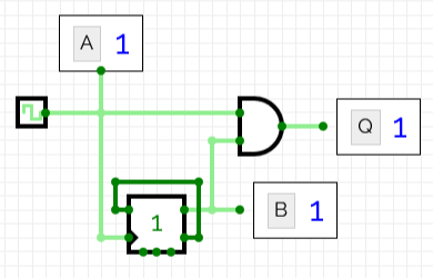
- Inputs are a clock and a D flip-flop:
- Clock turns off & on (adjustable via project properties)
- D flip-flop flips from off to on when clock falls (so creates 2x as long pulses)
Timing Diagrams
- Sequential circuits have behavior that changes over
time
- Some elements may trigger based on a change in voltage, rather than a particular stable voltage
- System state may depend on hidden internal variables
- Timing diagram shows how inputs/outputs change over time, but it doesn’t show hidden variables directly
- We’ll see more of these later
Designing Circuits
Designing Circuits
- Given a truth table, how to design a circuit for it?
- Use sum-of-products to build a Boolean expression
- Wire up gates for each operation
- Might be an inefficient circuit if you don’t simplify
- Gets messy w/ many inputs
Designing Circuits
- Can also use intuition, especially when building for many inputs
- Often, we have 8, 16, or 32 bits (= wires) to work with
- Just like trying integration rules in calculus, you can try out different operations over many bits mentally, and work towards a solution
Parity
- A parity bit is set so that the total number of ON bits in a message, including the parity bit, is even
- By sending a parity bit along with each row of a message, you can quickly determine if a row of the message has been corrupted (assuming only 1 bit is corrupted)
- Using row & column parity bits, you can often localize & correct errors
has 3 bits set, so the parity bit would 1
has 2 bits set, so the parity bit would 0
Parity with XOR
- It’s possible to design a circuit for the parity bit of a message using only XOR gates.
- The truth table for parity P on 2 bits A and B is the same as XOR.
- How to do this for more bits?
| A | B | P |
|---|---|---|
| 0 | 0 | 0 |
| 0 | 1 | 1 |
| 1 | 0 | 1 |
| 1 | 1 | 0 |
Bit Puzzles
Bit Puzzle Goals
- Exercise + grow your intuition about logical operators
- Learn some tricks that may eventually come in handy
- Gain a thorough understanding of 2’s-complement representation
C Bitwise Operators
& bitwise AND
| bitwise OR
^ bitwise XOR
~ bitwise NOT
! logical NOT: anything other
than 0 gives 0, 0 gives 1.
X << Y left-shift: shift
bit-pattern of X left by Y bits.
X >> Y right-shift: shift
bit-pattern of X right by Y bits.
Note: Left-shift adds zeros on right, right-shift adds copies of highest bit on left (or zeroes if unsigned).
Bit Puzzle Tips
- Work with 4-bit or 8-bit values; double-check with 32 bits
- Write out (by hand can be good) results from applying a few operators to see if you can see a pattern
Things to try:
- Complement the number
- Add or subtract 1
- Mask (
&with a mask value like0x0F) - !(0) = 1, but !(any other number) = 0
- Use XOR to compare values
- Bitwise OR a general solution with a special case
- Shift left & then right (or vice versa)