CS 240 Lab 4: ALU and Sequential Logic
Peter Mawhorter

How do Computers Work?

How do Computer Circuits Work?

  • Power flows through chips in the computer, creating patterns of activation driven by a clock and determined by logic gates.
    • Inputs like a keyboard feed into these patterns.
    • Some of these patterns drive outputs like a monitor.

How do Computers Represent Things?

  • High/low voltage patterns represent numbers in binary and/or symbols.
  • The computer performs basic operations with these numbers, like addition, through the use of specialized chips.
    • All other operations are built from a series of basic operations.

But what about… ?

  • Integrated circuits put together gates to perform various functions. Which circuits are used in a CPU, and what are their functions?
  • How can integrated circuits for several different functions be combined into a chip where we can select one function to apply?
  • How are clock signals generated & managed in the computer?
  • How is memory implemented using gates?
  • How can we change what a computer does by writing a program, instead of having to re-wire it?

How does the OS Work?

  • When you boot the computer, it launches an operating system, which provides control interfaces.
    • Usually there is graphical output and keyboard or touch input.
    • Servers are controlled remotely via text (a shell/terminal/command line).
  • OS allows user to launch programs, including custom programs.
    • Programs are files on the computer.

But what about… ?

  • How does the “boot” process work? Where does the operating system actually start?
  • What language does the “shell” use? Why are shells still around when we have graphical interfaces?
  • How does one program launch another? How does the OS keep track of programs that are running? How do two programs run at the same time?
  • How do compliers actually work? How does our text written in a programming language turn into a program, and what does a “program” actually consist of?

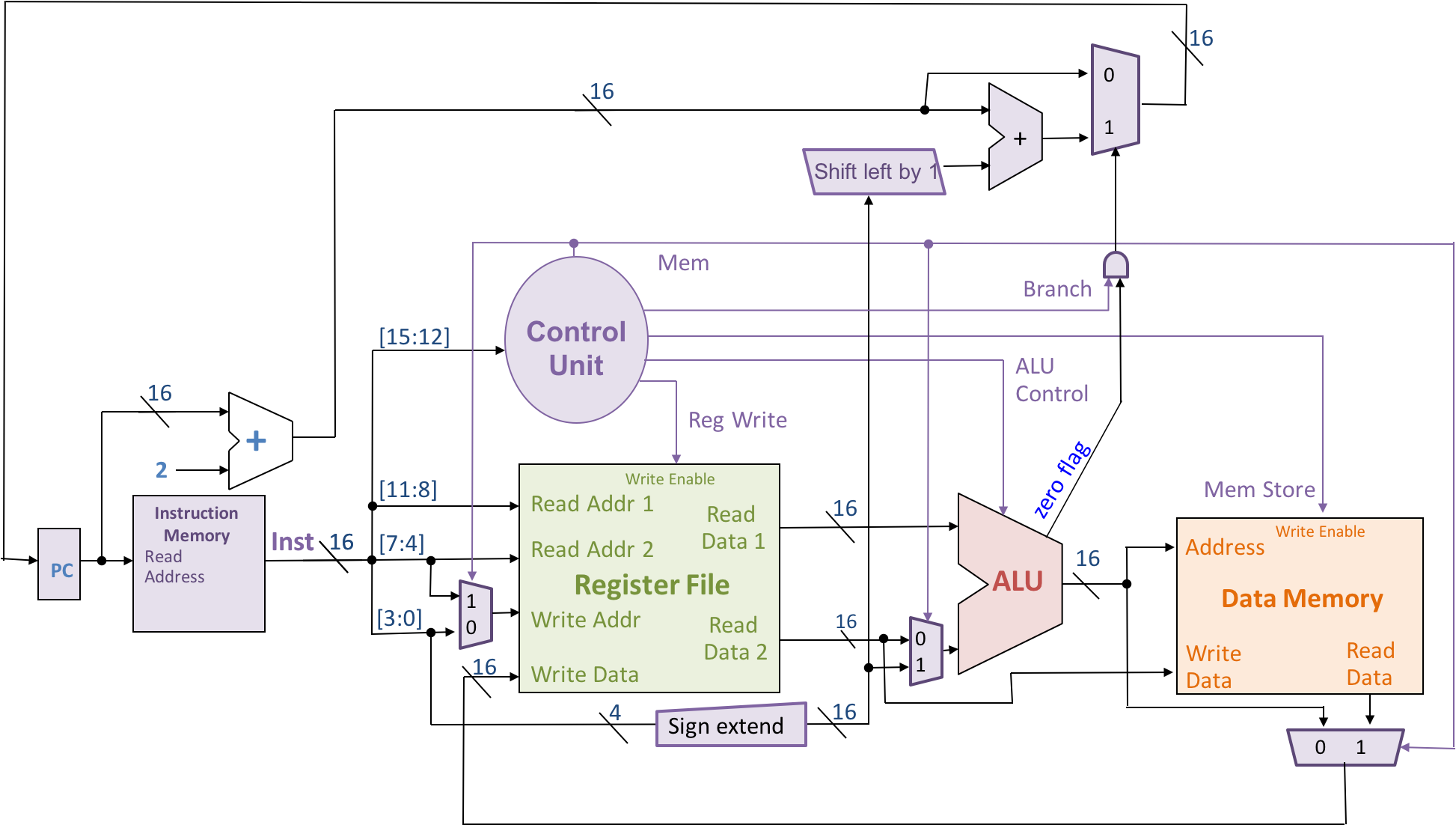
The datapath for the HW architecture. At the left, we start with the PC, which is a single register and which gets input from a line we’ll get to later called “PC input”. The PC feeds into the read address input of instruction memory, which outputs an instruction (16 bits) to the right. The PC also feeds into an adder whose other input is the number 2, and this gets forwarded to the branch-equal (or BEQ) mechanism. Back to the instruction, it gets split into bits 0-3, 4-7, 8-11, and 12-15. Bits 12-15 go to the control unit, drawn as a circle, which generates “Mem,” “Branch,” “Mem store,” “Reg Write,” and “ALU Control” outputs. We’ll see those pop up later, for now going back to the Instruction Memory outputs, bits 0-3 and 4-7 go into a 2x1 mux which feeds the write address of the register file, and which is selected by the “Mem” control signal. Bits 0-3 also bypass the Register file, go through a sign extender to become 16 bits, which we’ll call “offset.” This offset feeds into another 2x1 mux for the second ALU operand that’s also controlled by the “Mem” signal, as well as going to a shift-left-by-1 to become the second input to the first adder in the BEQ mechanism mentioned before. This BEQ mechanism adds the PC + 2 to the offset and then selects between that result and the original PC + 2 result using a 2x1 mux which is selected by an AND result combining the “Branch” control signal and the “Zero” output of the ALU. The result of that mux is the PC input mentioned right at the beginning. That wraps up destinations for the “offset,” backing up to the instruction bits, bits 4-7 also go to the Read address 2 for the Register file, while bits 8-11 go to the Read address 1. The only other Register file input is the Write Data, but we’ll get to that later. With two read addresses specified, along with a write address, the register file takes the “Reg Write” control signal as its “Write Enable” input, and outputs “Read data 1” and “Read data 2.” Read data 1 is 16 bits and goes straight in as the first operand of the ALU. Read data 2 (also 16 bits) is the second input to the mux described earlier that feeds the second ALU operand (whose other input if you recall is the sign-extended bits 0-3 of the instruction itself). Read data 2 is also forwarded to the Data Memory as its “Write Data” input (more on that in a second). This takes care of the outputs of the register file; with two operands to work with, the ALU also gets the ALU control signal from the control unit, and produces the aforementioned “Zero” output plus a 16-bit result. The ALU result serves as input to the Data Memory “Address” input, and also goes to a 2x1 mux below data memory which connects back to the “Write Data” input of the register file we mentioned earlier. That mux is controlled by the “Mem” signal from the control unit, and its other input is the “Read Data” output of the Data Memory, so either the ALU result or a piece of data whose address is specified by the ALU result will get written to a register file (if “Write Enable” is on, of course). As mentioned previously, the Data Memory also gets Write Data input from the Register File’s Read Data 2 output. It’s third and final input is a “Write Enable” which comes from the “Mem store” control unit signal. As already mentioned, its only output (“Read Data”) feeds into a mux and (if selected) back to the register file’s write input. And that’s the end of the datapath! 

The schematic diagram of the full CPU.

The CPU connections listed as a table:

Component Inputs Outputs
PC
  • Next Address from BEQ Logic
  • PC to read address of Instruction Memory
  • PC + 2 to next address for BEQ Logic
Instruction Memory
  • Read Address from PC
  • 16-bit Instruction splits into
    • Bits 12-15 go to the Control Unit
    • Bits 8-11 go to Read Addr 1 of Register File
    • Bits 4-7 go to:
      • Read Addr 2 of Register File
      • Register File Write Addr Mux
    • Bits 0-3 go to:
      • Register File Write Addr Mux
      • Sign extend to 16 bits and then:
        • ALU 2nd Operand Mux
        • Shift left 1 into Offset for BEQ Logic
Control Unit
  • Bits 12-15 of Instruction
  • Reg Write signal goes to Write Enable of Register File
  • ALU Control signal goes to control inputs of ALU
  • Branch signal goes to BEQ Logic Branch input
  • Mem Store signal goes to Write Enable of Data Memory
  • Mem signal goes to:
    • Register File Write Addr Mux
    • ALU 2nd operand Mux
    • ALU/Memory result Mux
Register File
  • Read Addr 1 from bits 8-11 of Instruction
  • Read Addr 2 from bits 4-7 of Instruction
  • Write Addr from Register File Write Addr Mux (either bis 0-3 or 4-7 of instruction)
  • Write Data from Final Result Mux (either ALU Result or Data Memory Read Data output)
  • Write Enable from Reg Write output of Control Unit
  • Read Data 1 goes to ALU 1st Operand
  • Read Data 2 goes to:
    • The ALU 2nd operand Mux (along with sign-extended instruction bits)
    • The Write Data input for Data Memory
Arithmetic Logic Unit (ALU)
  • 1st operand from Read Data 1 of the Register File
  • 2nd operand from the ALU 2nd operand Mux (either Read Data 2 from the Register File or bits 0-3 of the instruction after sign extension to 16 bits)
  • ALU Control output from Control Unit
  • 16-bit result goes to:
    • Address input for Data Memory
    • Final Result Mux (along with Read Data from Data Memory)
  • Zero flag goes to Zero input to BEQ Logic
Data Memory (RAM)
  • Read Address from ALU result
  • Write Data from Register file Read Data 2 output
  • Write Enable from Control Unit Mem Store signal
  • Read Data result goes to Final Result Mux (along with ALU result)
BEQ Logic
  • Next Address from PC + 2
  • Offset from bits 0-3 of instruction after sign extend and shift left by 1
  • Branch from Control Unit
  • Zero from ALU Zero Flag
  • Adds PC + 2 and Offset inputs and then selects that result or the original PC + 2 result using an AND between the Branch and Zero inputs. Takes this result as the Next Address and feeds it back to the PC.

What we’ll see today

  • How can integrated circuits for several different functions be combined into a chip where we can select one function to apply?
  • How are clock signals generated & managed in the computer?
  • How is memory implemented using gates?

Outline

Arithmetic Logic Unit

Arithmetic Logic Unit

  • A multi-function circuit that operates on binary values A and B producing a result R.
  • 2-bit Op1/Op0 inputs select the operation: AND, OR, or +
    • NOR and - can be achieved using invertA and negateB
    • invertA just inverts each bit of A
    • negateB inverts each bit of B, and also sets the CarryIn bit

Arithmetic Logic Unit

  • Has CarryOut, Sign, Overflow, and Zero outputs in addition to the output bits R
    • CarryOut is the carry-out from addition (still present when a different operation is selected)
    • Sign is just the highest bit of R
    • Overflow is true when there’s two’s-complement overflow
    • Zero is true when all of the R bits are zero

Arithmetic Logic Unit

invA negB Op1 Op0 R
0 0 0 0 A AND B
0 0 0 1 A OR B
0 0 1 0 A + B
0 1 1 0 A - B
1 1 0 0 A NOR B

(other combinations are possible)

Arithmetic Logic Unit

An ALU symbol (trapezoid with a triangle cut out of the longer side) that has a pink heart drawn in the middle. 

The ALU is the heart of the computer: everything a computer does is a transformation of data, and the ALU is what performs those transformations.

Memory

Memory

  • Need to store + retrieve values for the ALU to work on
  • An SR latch can be “set” or “reset”
  • A D latch stores one bit of “data”
  • A D flip-flop reads only on the clock edge

Bistable Circuits

  • Until now, we solved for voltage
  • A bistable circuit has two different voltage patterns that are equally stable.
    • Must use assumptions to solve for voltage
    • Look for two different solutions

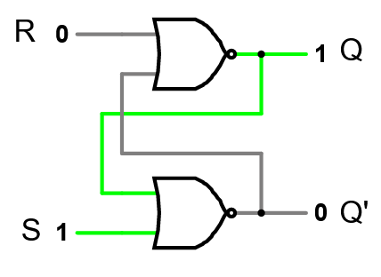
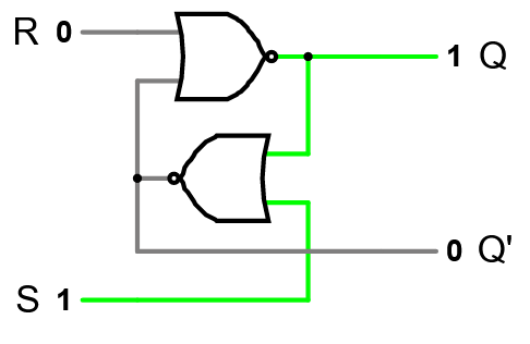
SR Latch

  • S sets the latch (Q=1)
  • R resets the latch (Q=0)
  • Q and Q’ should be opposites
    • Both are off when S=R=1
  • When S=R=0, it remembers
  • Race condition going from S=R=1to S=R=0

SR Latch Alternates
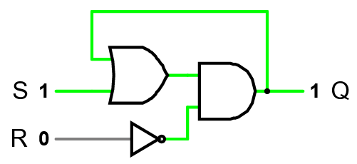
An SR latch created using an OR gate, and AND gate, and a NOT gate. The S signal feeds into one input of the OR gate, whose output feeds into the AND gate. Meanwhile, the other input of that AND gate is connected to the R input, but with a NOT gate on the way. The output Q is the output of the AND gate (there is no Q’ output for this diagram). The output Q is also fed back into the other input of the OR gate that S connects to. 

Simulation link (AND/OR version)

(This version is more stable)

Clocks

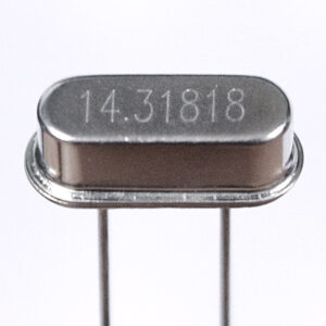
An rectangular metal package with rounded ends, with two metal connecting pins coming out of the bottom. The top is embossed with the number 14.31818. This is a 14.31818 MHz crystal resonator. 

  • Need to synchronize circuit changes
  • Want some parts to activate only when selected
  • A “clock” input can be either of these
  • Has to change from +5V to 0V quickly
  • Needs to be distributed to all parts of the processor
  • Can use ~30% of the power in a CPU

Clock Signals
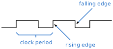
A diagram of a clock signal. It shows a black line which moves up and down in rectangular segments as it goes from left to right, always at the same high or low height. A raised segment plus the following lowered segment together form a “clock period.” The raised and lowered segments aren’t necessarily the same length (in this picture the ratio is 3 raised to 2 lowered). When the signal moves from low to high, that’s the rising edge, and when it moves back low, that’s the falling edge. 

  • In each cycle the clock is on for a time and then off for a time
  • When the signal changes, that’s a rising or falling edge
  • The period is the time between rising edges
  • The frequency of the clock is 1/period

Clocked SR Latch
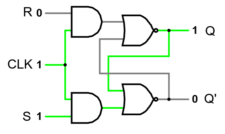
  • When clock is off, latch remembers
  • When clock is on, set and/or reset inputs can go in
  • “Clock” may really be “write”
  • Now if S=R=1 and we turn the clock off, we easily trigger the race condition

D Latch
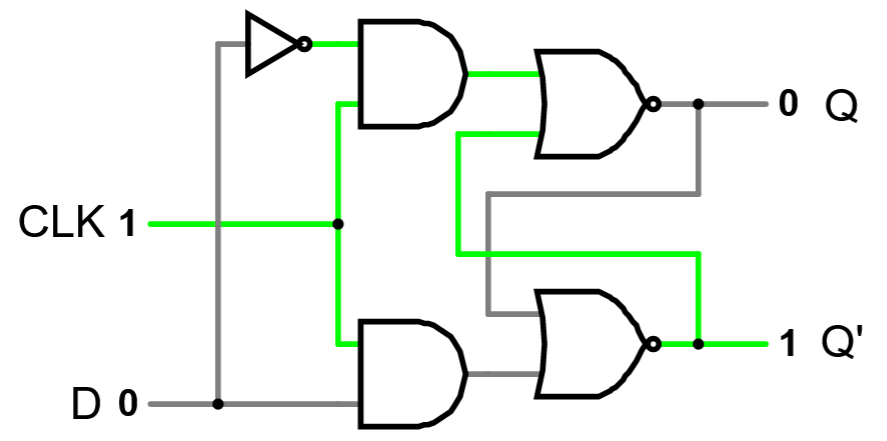
  • When D is high, we have S=1 / R=0
  • When D is low, we have S=0 / R=1
  • S=R=1 is impossible
  • S=R=0 only when clock/write is low

D Flip-Flop
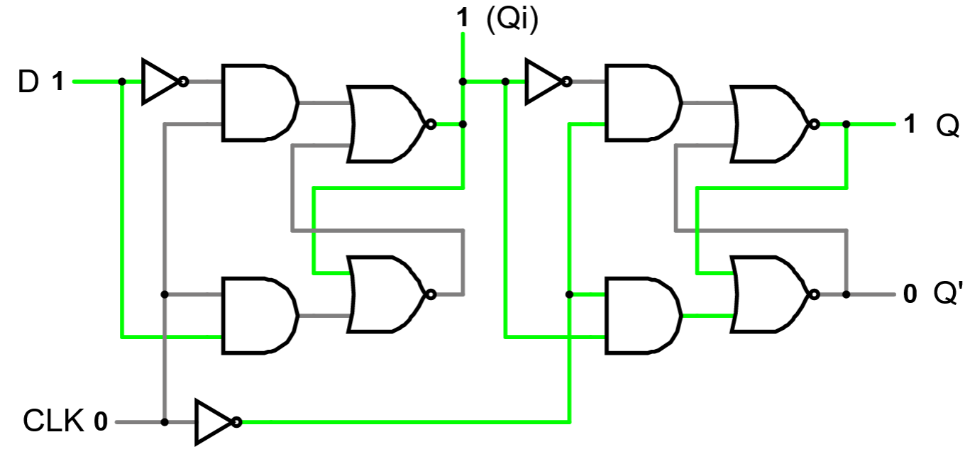
  • Captures state of D at falling clock edge
  • Broadcasts old D value during entire clock ON pulse

Flip-Flop Timing

  • Clock goes ON (rising edge)
    • ALU etc. start their work to get results
    • Have until the end of the clock pulse to settle
    • Flip-flops still broadcast previous-cycle results
  • Clock goes OFF (falling edge)
    • Flip-flops capture new results
    • Stuff can settle down until next rising edge

Remember that “clock” could be “write data pulse.”

Memory Organization

Register Files

  • Multiple D flip-flops make up a register
    • Common clock input; different data inputs/outputs
  • A register file has multiple registers
    • Multiplexers & decoders select register(s) to write/read
    • Often has 2 output blocks & one input block since ALU needs 2 inputs and has 1 output each cycle.

RAM

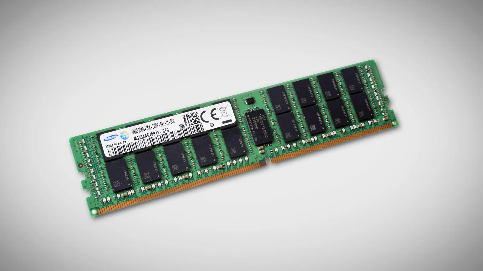
  • Random Access Memory or RAM stores lots of data
    • Organized into n-bit words of data
    • Each word has an address
    • Same mechanisms as a register file
    • Different tech (bigger/slower/cheaper)