Circuit Divination
- Due: 1:30pm Friday, 25 September
- Submission: turn in a paper copy in class
- Reading: SCO 3.1 - 3.3
- Collaboration: This assignment follows the standard collaboration policy. You may discuss problems and high-level strategies with other students, but your solutions must be your own work. You must cite anyone with whom you discussed the problems at the top of your submission.
- Circuit Divination title courtesy of Sam Mincheva ‘17, CS 240 S’15.
1. Marauder’s Map
Draw a Karnaugh Map for the function F defined by the truth table below. Use the Karnaugh Map to derive a minimal sum-of-products Boolean formula for F. Show any intermediate work.
| A | B | C | D | F(A,B,C,D) |
| 0 | 0 | 0 | 0 | 1 |
| 0 | 0 | 0 | 1 | 1 |
| 0 | 0 | 1 | 0 | 1 |
| 0 | 0 | 1 | 1 | 0 |
| 0 | 1 | 0 | 0 | 0 |
| 0 | 1 | 0 | 1 | 1 |
| 0 | 1 | 1 | 0 | 0 |
| 0 | 1 | 1 | 1 | 1 |
| 1 | 0 | 0 | 0 | 1 |
| 1 | 0 | 0 | 1 | 0 |
| 1 | 0 | 1 | 0 | 1 |
| 1 | 0 | 1 | 1 | 0 |
| 1 | 1 | 0 | 0 | 0 |
| 1 | 1 | 0 | 1 | 1 |
| 1 | 1 | 1 | 0 | 0 |
| 1 | 1 | 1 | 1 | 1 |
2. Switching Network
Implement a switching network circuit that has two data inputs (A and B), two data outputs (C and D), and a control input (S). If S is 1, the network is in pass-through mode: C should equal A and D should equal B. If S is 0, the network is in crossing mode: C should equal B, and D should equal A
3. Fixing the ALU
Background
In class, we designed a 32-bit ALU, built by connecting 32 1-bit ALUs of the following design:
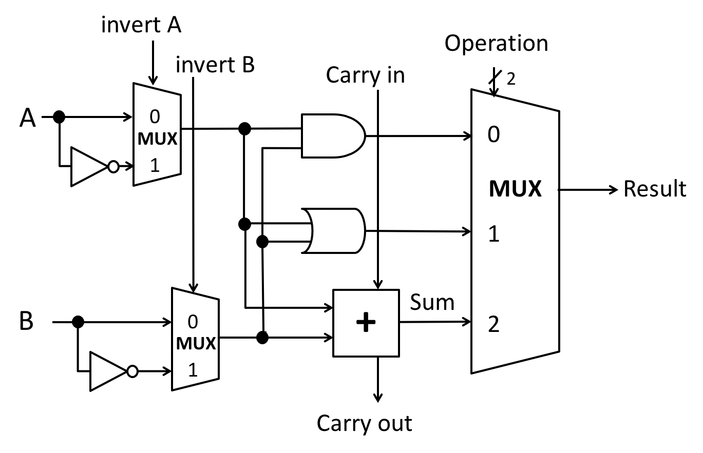
Between class and lab, we examined many relevant details of the 1-bit and full n-bit ALUs. Recall that:
- The carry out from each bit is wired to the carry in of the next bit, if present.
- The full n-bit ALU has 4 lines of control input:
- invert A controls the invert A inputs of all of the 1-bit ALUs.
- negate B controls:
- the invert B inputs of all of the 1-bit ALUs; and
- the carry-in of the least significant bit ALU. (Saw this in lab, not in lecture.)
- Two bits of operation ID control the operation ID inputs of all of the 1-bit ALUs.
- We discussed how to implement the zero flag, sign flag, and carry flag condition codes as extra 1-bit outputs from the n-bit ALU.
Problems
We added several features to the ALU using minimal or no additional logic. However, some of our additions were incomplete. You will improve the ALU in the exercises that follow to fix these additions.
- Use the same design, but consider a 4-bit ALU for simplicity.
- When asked to draw additional logic, label inputs to your logic with text clearly describing where the inputs connect to wires in the original ALU. Alternatively, draw the full ALU plus your extensions.
- Write at most a short paragraph when asked for prose descriptions.
Complete the following exercises:
-
Design a circuit that implements the Overflow Flag condition code as a 1-bit output of the full n-bit ALU. Use minimal additional logic, i.e, the smallest number of extra gates. The output should be 1 if a two’s-complement overflow condition has occurred and 0 otherwise. Your additional logic may take any values avilable on any wires in the ALU as inputs.
- Draw the additional logic required.
- Explain how your circuit works in a few sentences at most.
-
We discussed how to implement a less-than check for two’s-complement operands. We simply performed A - B and then checked the sign bit of the result.
- Describe why this approach seems to work at first glance. For example, consider checking if A < B for A = -310 =
1101and B = 210 =0010. - Consider A = -710 =
1001and B = 610 =0110. Unfortunately, our ALU will claim that -7 < 6 is false! Explain why. - Reimplement less-than so it works correctly for all pairs of 4-bit two’s-complement operands.
- Show the values to set on each of the 4 control lines of the full ALU.
- Draw any additional logic necessary to compute the correct less-than result as a 1-bit output of the full ALU, yielding 1 if the less-than property holds and 0 otherwise.
- Describe why this approach seems to work at first glance. For example, consider checking if A < B for A = -310 =
-
Must we also fix our implementation of the equality test or is it already correct? Why?
4. Memory Construction
Complete ONE OF the two problems below. You may complete both for extra fun or extra practice, but no extra credit will be awarded for completing a second. (We will cover RAM concepts on Tuesday, 22 September.)
-
Construct a 256x8 SRAM by adding minimal logic to two identical 256×4 SRAM components.
- Treat the existing 256x4 SRAMs as indivisible elements with 4 data-in lines, 4 data-out lines, a set of address lines, and a write-enable line.
- Your resulting 256x8 SRAM should have 8 data-in lines, 8 data-out lines, a set of address lines, and a write-enable line.
- Assume that all registers inside the memory are edge-triggered (just like the registers used in lecture).
- Assume that, for both the existing SRAM and the one you build, memory is always reading unless the write-enable line is asserted (=1). (In other words, do not implement a chip-select line.)
- Do not draw each individual line in a bus unless necessary to distinguish their endpoints. Instead, use the hatch marks and width annotations we have used when diagramming similar circuits in class.
-
Build a 64K x 8 SRAM by adding minimal additional logic to an underlying 16K x 32 SRAM. Carry over the same types of inputs, outputs, and assumptions as in part (a), adjusted for these new dimensions.
- Unlike in part (a), the underlying memory component in this problem has the same capacity as the final product, but different dimensions:
- The addressable unit of data (i.e., the size of each memory location) is larger in the internal SRAM than in the SRAM you will build (32 bits vs. 8 bits).
- There are fewer memory locations in the internal SRAM than in the SRAM you will build (16K vs. 64K).
- Be careful with writes: when writing an 8-bit value into your memory, you must be sure not to destroy the other 24 bits that share the same underlying 32-bit cell.
- Unlike in part (a), the underlying memory component in this problem has the same capacity as the final product, but different dimensions: