CS 240 Lab 1: Transistors to Gates

Peter Mawhorter

Outline

Course Structure

Important Policies

  • No food or drink
    • You may step out for a snack/sip, and we’ll have a break.
  • Masks are expected
    • Asymptomatic infections mean that we will very likely have someone who is infectious in lab this semester, and even they won’t know it.
    • COVID-19 comes with a significant risk¹ of long-term (presumably permanent) symptoms which interfere with activities of daily living.
    • Some students & professors at Wellesley are immunocompromised and cannot receive full protection from vaccines.

1: This risk is hard to quantify, but many studies suggest it is somewhere between 1/1000 and 1/10 (i.e., between 0.1% and 10%). This planned study has a good discussion and citations, in particular, the 4th paragraph of the “expected key results” section. The risk is significantly higher than for the flu.

Course Parameters

  • Pre-lab exercises in Gradescope
    • Pre-lab exercises are individual
    • Review slides & attempt exercises before lab
    • Revise exercises after lab
  • I will assign different partners each lab
    • Let me know if you have preferences
  • Grades are self-assigned for each unit based on pre-lab feedback and per-lab reflections
    • I may negotiate your grade if it seems wrong

Partner Work

  • Be kind to each other (yes, even when you’re tired)
  • Enhance each others’ learning
  • You’ve had practice at this

Expectations

  • You’re now full-fledged CS majors
    • Capable of independent learning
    • Will ask questions when you need to
    • Will be responsible for meeting deadlines, doing prep work, etc.
  • You will succeed and thrive in this class, and you’ll go on to do great things with this knowledge.

Growth Mindset

  • When you’re having trouble, identify why and what you need to practice to improve.
  • Don’t limit your own potential by buying into the belief that you are either “bad at” or “good at” a subject.
  • This class is hard in order to make you grow strong (but hopefully in a gentle way).

Logging In

  • Use your Wellesley username/password for Windows
  • Use your CS Department username/password for Linux
  • Keep pressing F12 (about 1 Hz) when it boots to get to the boot menu for some machines

Setup

  1. Find your partner.
  2. Log in to Windows on at least 1 machine.
  3. Open up a browser an navigate to the class website’s lab section.
    • Scroll down to find Lab 1
    • Open up the learning goals, slides, and notebook

Basic Electronics

What is Electricity?

  • Electricity = the movement of electrons in a material
    • Movement happens because of extra electrons in one place, or extra “holes” in another place, or both.
    • Electrons are so fast. Really, just so fast.

What is Electricity?

  • We measure the surplus or deficit of electrons in relative terms
    • This is voltage (V, measured in Volts), and is always a difference between two points.
    • When unimpeded, the flow of electrons quickly reduces voltage to 0.
  • Rate of flow is called current, (I, measured in Amps)
  • All materials resist the flow of electrons
    • This is called resistance (R, measured in Ohms = Ω)

What is Electricity?

  • Materials that have low resistance are called “conductors”.
    • The resistance of a copper wire is basically 0 (it’s around 1 Ω per 1000 feet of wire, depending a bit on thickness).
  • We use resistors with specific Ohm ratings to create resistance in our circuits, often ~1.8 kΩ.
  • Your body has a resistance value anywhere from 300-100,000 Ω
  • Air has resistance of 1.3-3.3×10¹⁶ Ω (until about 21 kV/cm)

Ohm’s Law

V=I×RV = I \times R

Voltage (V) equals current (I) times resistance (R).

  • More voltage → more current
  • More resistance → less current, since I=VRI = \frac{V}{R}
  • Zero resistance = infinite current (!)

A diagram showing positively and negatively charged materials, with current as the flow of electrons from the negatively-charged material to the positively-charged material. A second diagram showing a 5-volt voltage source with positive and negative terminals. The positive terminal connects to a 250-Ohm resistor, and then back to the negative terminal in a loop. The diagram indicates that 0.2 amps of current are flowing from the positive to the negative terminal. 

Ohm’s Law

  • Conventions are hard to change, current is shown backwards from the flow of electrons (we don’t care).
  • For our purposes, an open switch (meaning electricity has to jump across air) has infinite resistance: no current flows.
  • We also don’t care about the resistance of our wires, they are effectively 0.
  • A “short circuit” means a circuit with negligible resistance. Current becomes very high, until the circuit destroys itself.

Digital vs. Analog

Analog

Analog circuits like antennas or speakers have a complex balance of resistance, current, and voltage, which varies over time.

Digital

We will study digital circuits, which have defined “high” and “low” voltage values; the exact numbers don’t matter so much.

Digital vs. Analog

  • A typical digital circuit uses just 5 volts, and might define “high” as anything above 3 volts, and “low” as anything below that (more detail).
  • Only minimal current may be necessary for the circuit to function, as long as the correct voltage differences can be achieved.
  • Using “high” and “low” we can represent True and False, or 1 and 0.

(Once you give a computer scientist a 1 and a 0, it’s game over.)

Prototyping Workbench

A picture of a prototyping workbench, with some transistors, wires, and chips connected. The power switch is on the upper left, and is a red rocker-type switch which is ON when the top part is pushed down and OFF when the bottom part is pushed down. Black and red wires are connected already which connect +5V and ground to 6 sets of vertical rails going up and down the center, which is white. Each rail connects vertically underneath a series of holes which can be used to plug wires into it. In between these sets of rails are three sets of paired rows of holes, where in each row has a left and right half. The two halves are not connected to each other, but every hole on each half is connected to the other holes in the same half of the row. This allows a chip to be inserted spanning between the halves, such that each pin of the chip connects to a single row on either the left or right half. This in turn makes it easy to plug up to 4 wires into holes that will connect to a particular pin of the chip (the half-rows have 5 holes each, and the chip leg takes up one of them). Two chips are plugged into the board in this manner in the upper-right region. On the left, two transistors are plugged in, spanning across several rows. Outside the center region with the holes, there are input and output devices around the edge of the board. A function generator below the power switch on the left, two push-buttons below that, a BNC J1 connector on the bottom-left, a series of eight logic switches to the right of that bottom-left corner, 10K and 1K POT connections in the middle of the bottom, S9 and S10 switches on the right of the bottom, a BNC J2 connector on the bottom-right, an 8Ω speaker above that on the right edge, and a set of 8 logic indicator lights on the upper part of the right edge. At the top-right there are three voltage connections (+5V, +13-15V, and -13-15V) and a ground connection, with two adjustment knobs at the top. Each of these various input/output devices has its own set of holes into which wires can be connected, the push-buttons are already connected to the left-most +5V rail with resistors, and the 8 logic switches have been wired to 8 of the horizontal rows on the bottom-left of the board. 

A prototyping workbench has places to hold wires and chips so you can put them together easily, with internal horizontal and vertical connections. It also has a power supply and things like switches and LEDs built-in.

One of our older-model workbenches, with voltage & ground sources at the top right, logic indicators below that, push buttons at the bottom left, logic switches below and slightly right from the push buttons, and a big area of protoboards in the middle. Voltage and ground sources are red and black colored knobs; logic indicators are 8 little LED lights with plastic sockets for connecting to them; push buttons are buttons that pop back out when you release them, along with plastic connector sockets, and logic switches are switches that can be toggles on or off, with plastic connector sockets. The protoboards are pieces of white plastic with lots of sockets in them: two columns of sockets down each side, and many rows of sockets split into two half-rows in the middle. Each socket is just big enough to plug in the tip of one of the wires we’re using. There are 6 protoboards packed edge-to-edge in a 3-wide-by-2-high setup; each is taller than it is wide so the whole setup is squarish (but slightly taller than it is wide). 

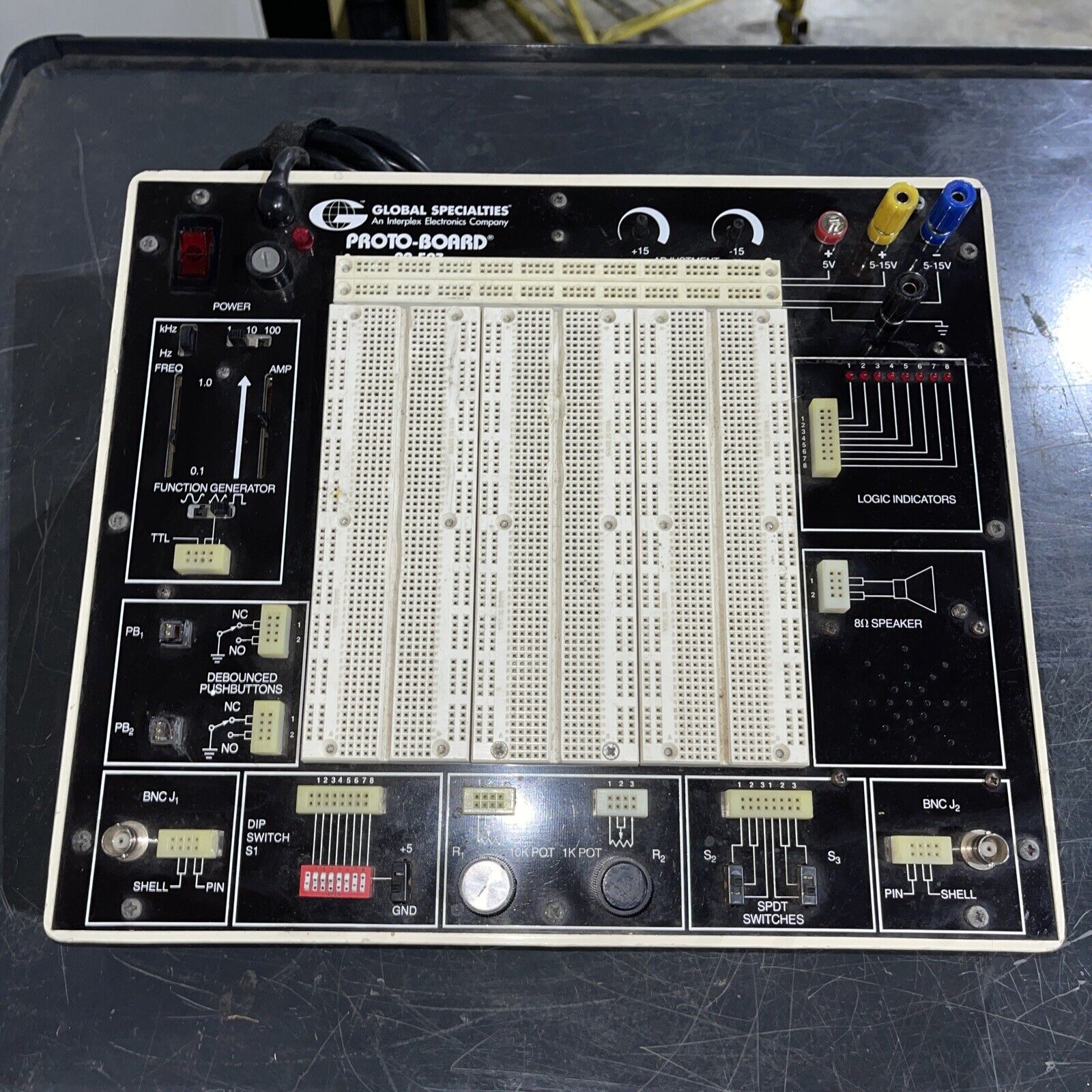
This is one of our older model workbenches. The next few slides show which components we’ll be using in this class.

The central white area with lots of small sockets is where we’ll attach chips and wires to build our prototypes. Wire tips and the pins of chips should fit snugly into the sockets.

Smaller socket groups around the edges connect to pre-mounted components.

The same picture, with horizontal and vertical connections highlighted: of the six proto-boards in the middle area, one is highlighted, and the two vertical columns of sockets on its left edge are shown as connected. Similarly, on the left side of the highlighted board, the first 6 5-socket rows are shown as connected. 

Internally, each row of 5 sockets is connected horizontally, so that components plugged into the same row are in contact. There are also 12 columns of sockets that aren’t part of the 5-socket rows. Each of these columns has internal vertical connections, so that the entire column is connected.

A few of the relevant connections are shown at left; the same pattern applies throughout.

The workbench again, now showing voltage and ground connections. The +5V and GND plugs at the upper-left of the board are circled, and the horizontal socket strips for each along the top are indicated with lines (the +5V strip is the topmost two rows of sockets on the bench, and the next two rows are GND rows). From these strips, lines are drawn vertically down each of the connected columns in the protoboard section, indicating how our workbenches are pre-wired to distribute power and ground connections. Specifically, for each of the 6 pairs of vertical rails, the left-hand rail is connected to +5V and the right-hand rail is connected to ground. 

We have set up small red and black jumper wires to distribute power and ground connections throughout the board from the top strips.

Each pair of vertically-connected columns has +5V on the left and ground on the right. This makes it easy to supply voltage or ground at any point on the board by connecting a horizontal row to one of the nearby vertical rails.

The workbench again, now showing the logic indicators on the upper right side. These are 8 LEDs with lines indicating their connection to horizontal pairs of sockets in a 2x8 socket strip. The first LED is connected to the top pair of sockets, and the rest are connected to subsequent lower sockets. 

The logic indicators on the upper right can be used to display whether the connected wire has high or low voltage. If the LED is on that means the voltage is high, if it’s off that means low. (The newer models have two LEDS to indicate high/low separately.)

Connecting to either of the two horizontal sockets corresponding to a particular LED will supply voltage to that LED.

The workbench again, now showing the logic switches at the lower left. These are 8 switches that can be toggled between on an off states. Lines on the board indicate their connections to pairs of vertical sockets in an 8x2 socket strip above them. 

The logic switches near the lower left corner of the board can be toggled on or off. When on, they supply +5V power to the two corresponding sockets in the nearby strip. When off, those sockets are disconnected.

This picture doesn’t show it, but in our lab, these are pre-connected to ground through a high-resistance resistor. This means that when the switches are off, they will be low-voltage instead of disconnected.

The workbench again, now showing the push-buttons at the lower left. These are 2 buttons each connected to 2x4 socket strips. The ‘on’ state of the button controls the upper 4 sockets in the corresponding strip. 

The push-buttons in the lower left work like switches, except that they bounce back to off when released. When off, the top 4 sockets of the nearby strip are grounded, when on, the bottom 4 are grounded instead.

Not shown here, in our lab one of the top sockets for each button is connected to +5V via a resistor. This means that when the button is pressed, the top 4 sockets will be high-voltage, and when it’s released, they’ll be low.

Transistors

Transistors

  • To be able to build NOT, AND, and OR gates in a circuit, there has to be a way for voltage or current in one place to manipulate the flow of current or the difference in voltage somewhere else: a switching mechanism.

  • Early switches were big (vacuum tubes) but transistors represent the culmination of decades of research into making them smaller.

  • A modern transistor can be as small as 5 nanometers, with 10s of billions packaged on a singe chip.

Transistors

  • When voltage is present at the trigger side of a transistor, current may flow through, but if no voltage is present, current may not flow.
  • To create a NOT gate, connect input A to the trigger, and output F to the wire leading into the transistor’s channel. (simulation link)
    • When A is high, the current flows across the transistor, draining away voltage above the transistor.
    • When A is low, current cannot pass the transistor, and gets bottled up behind it, creating high voltage at the output.
    • Resistors prevent a short circuit in either state.

An image showing how transistors can be used to create NOT, NAND, and AND gates. TODO 

An image showing how transistors can be used to create NOR and OR gates. TODO 

Building a Gate

  • A NOT gate can be built with 2 resistors and 1 transistor:
    1. Connect one resistor to the top/input leg of the transistor, and then to the +5V rail of the board.
    2. Connect the same horizontal row that has the resistor and transistor input plugged in to one of the “logic indicator” sockets using a wire. This is the gate output.
    3. Connect the middle/trigger leg of the transistor to one of the push-buttons (they already have resistors connected, so you get one resistor for free).
    4. Connect the bottom/output leg of the resistor to the ground rail on the board.
  • Double-check your connections, then turn on power to the board. The logic indicator should read “high.”
    • Push the button to change the indicator to “low.”

Integrated Circuits

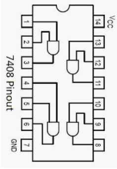
  • Integrated Circuits (i.e., chips) contain transistors in a specific configuration.
  • The pinout for a chip specifies the internal wiring. Find them online based on the chip number, or in the TTL Data Book.
  • Must be connected to both a voltage source and ground to work.

A picture of an integrated circuit. The main body is black with faint grey writing on it that says the part number and the manufacturer. Sticking out on each side are silver metal spikes or legs (this one has 7 on each side). These point downwards, and can be plugged into the grid of holes in our protoboards. One end of the chip has a small semicircle cut out to help figure out which end is which (we call this end the “top”). 

Integrated Circuits

  • Pins are numbered starting with 1 at the top-left and going around counter-clockwise.
  • Notch determines the “top.”
  • Watch out: the pins are often shown lined up in diagrams, rather than wrapped around the chip.

A pinout diagram for the “7408” chip, with 14 pins, 7 on each side. Internally, it contains AND gates: pins 1 and 2 are inputs to an AND gate with output to pin 3, and similarly for pins 4/5 to 6, pins 9/10 to 8, and pins 12/13 to 11. Pin 14 (at top-right) is labelled Vcc (for Voltage at Common Collector; we just want +5 volts here). Pin 7 (at bottom-left) is labelled GND, for ground. 

Thinking Logically

Gates and Truth Tables

  • A truth table specifies the high/low or 1/0 combinations for different parts of a digital circuit. (You saw these in CS 111 for Booleans)
  • True = 1 and False = 0
  • Here, two inputs A and B (called literals) are shown, along with a function F of A and B.
    What function is this?
A B F
0 0 0
0 1 0
1 0 0
1 1 1

Boolean Algebra

  • Before, you might write “A and B” or “A && B,” now we will write just “ABAB” for AND and “A+BA + B” for OR.
    • Basically, AND is multiplication and OR is addition.
    • 1×11 \times 1 is 1, but anything ×0\times 0 is 0.
    • 0+1=1+0=1+10 + 1 = 1 + 0 = 1 + 1 (if you can’t go above 1).
    • Use ’ for NOT, or write a bar above: A’ or A¯\overbar{A}

Boolean Algebra

  • A minterm is an AND of all of the inputs to a function, possibly with NOTs. The four minterms of two inputs A and B are: AB, A’B, AB’, and A’B’.
  • A maxterm is an OR of all inputs, possibly negated. The four maxterms of two inputs A and B are:
    A + B, A’ + B, A + B’, and A’ + B’.

Basic Functions

Here are truth tables for NOT, AND, and OR, which you are already familiar with:

NOT
F = A’
A F
0 1
1 0
AND
F = AB
A B F
0 0 0
0 1 0
1 0 0
1 1 1
OR
F = A + B
A B F
0 0 0
0 1 1
1 0 1
1 1 1

Basic Functions

Here are truth tables for NAND, NOR, and XOR:

NAND
F = (AB)’
A B F
0 0 1
0 1 1
1 0 1
1 1 0
NOR
F = (A + B)’
A B F
0 0 1
0 1 0
1 0 0
1 1 0
XOR
F = AB’ + A’B
A B F
0 0 0
0 1 1
1 0 1
1 1 0

Basic Functions

  • Why NAND, NOR, and XOR?
    • NAND and NOR are easier to build in a circuit than AND and OR, as we’ll soon see.
    • XOR is quite useful in a number of applications, including cryptography.
    • As the formulas show, NAND, NOR, and XOR can be built out of AND, OR, and NOT.
    • Alternatively, AND and OR can be built from NAND, NOR, and NOT.

Gate Symbols

A diagram showing the circuit symbols for each gate: a flat back and round head for AND, a curved back and pointy-but-curved head for OR, and a triangle with a dot at the tip for NOT. For NAND and NOR, the symbol is the same as AND and OR, but with a dot added to the tip. XOR is the same as OR, but with an extra curved line before the gate, crossing through both input wires and parallel to the curved back of the gate. Except NOT, each gate has 2 inputs and 2 output, NOT has 1 input and 1 output. 

Aside: Mental Juggling

Aside: truth tables present information clearly, but they’re hard to read, and it’s harder to keep them in your head as you then try to apply them to each other or think through a circuit.

This class will repeatedly strain (and also develop) your ability to mentally juggle multiple steps of translation between different representations and parts of a system.

Aside: Mental Juggling

Use tools to improve your juggling skills:

  • Keep references handy, ideally visible without having to even click or turn a page.
  • Practice to internalize key info, like the basic truth tables.
  • Keep scratch paper or a scratch file handy to write things out when your mental stack is out of space.

Sum-of-Products

  • Sum-of-products is a fancy way of saying: read the truth table and make an AND out of each line where the output is 1, then OR those together.
    • Remember that AND = multiply (i.e., product), and OR = add (i.e., sum).
    • Each product is a minterm.
  • For this table, there are three 1s for F, with minterms A’B, AB’, and AB, so the sum-of-products form is F = A’B + AB’ + AB.
A B F
0 0 0
0 1 1
1 0 1
1 1 1

Sum-of-Products

  • Any boolean function can be expressed as a sum-of-products, which only needs NOT, AND, and OR.
  • If we had circuits that could produce these functions, we could put them together to compute anything.

Equivalence

Two functions with the same truth table are equivalent.

F = A’B’ + A’B
A B A’B’ A’B A’B’ + A’B
0 0 1 0 1
0 1 0 1 1
1 0 0 0 0
1 1 0 0 0
Q = A’ + A’B + A’B’
A B A’ A’B A’B’ A’ + A’B + A’B’
0 0 1 0 1 1
0 1 1 1 0 1
1 0 0 0 0 0
1 1 0 0 0 0

Equivalence

  • Use Boolean algebra to find/prove equivalence.
  • Find ways to make the same circuit with fewer or cheaper gates.