
🔬 Lab
CS 240 Lab 2
Data as Bits
CS 240 Lab 2
Data as Bits
In lab today, you will continue to learn about digital logic, and how bits are used to represent data. You will experiment with Boolean functions and basic gates, including some investigation of binary numbers. Some of the exercises will involve building physical circuits on your protoboard, as we learned to do last week. You will also use a simulator to simulate some circuits.
In the final exercises, you will begin to explore how to think about and solve bit puzzles.
Exercise 1: Binary Circuits
Hexadecimal representation is often used in place of or in conjunction with binary representation when working with binary numbers. This is because hexadecimal is more concise than binary, but is easy to convert to/from binary, since both bases (2 and 16) are powers of two. So, a single digit in hexadecimal is always a 4-digit value in binary, as follows:
| Hex | Binary | |||
|---|---|---|---|---|
| QD | QC | QB | QA | |
| 0 | 0 | 0 | 0 | 0 |
| 1 | 0 | 0 | 0 | 1 |
| 2 | 0 | 0 | 1 | 0 |
| 3 | 0 | 0 | 1 | 1 |
| 4 | 0 | 1 | 0 | 0 |
| 5 | 0 | 1 | 0 | 1 |
| 6 | 0 | 1 | 1 | 0 |
| 7 | 0 | 1 | 1 | 1 |
| 8 | 1 | 0 | 0 | 0 |
| 9 | 1 | 0 | 0 | 1 |
| A | 1 | 0 | 1 | 0 |
| B | 1 | 0 | 1 | 1 |
| C | 1 | 1 | 0 | 0 |
| D | 1 | 1 | 0 | 1 |
| E | 1 | 1 | 1 | 0 |
| F | 1 | 1 | 1 | 1 |
Note the patterns in this truth table:
- The least significant bit of the 4-bit value QA toggles every number.
- The next-least-significant bit QB toggles every other number.
- The QC toggles every four numbers.
- The QD toggles every eight numbers.
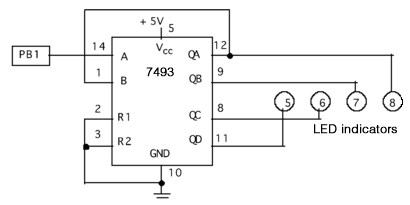
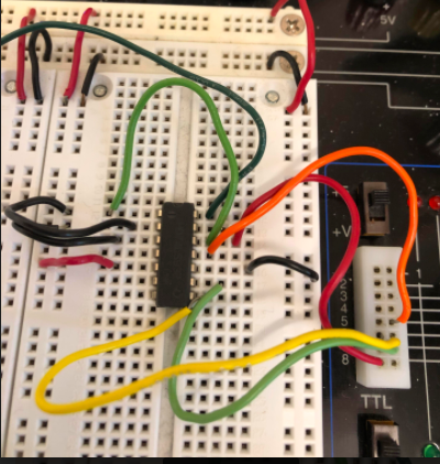
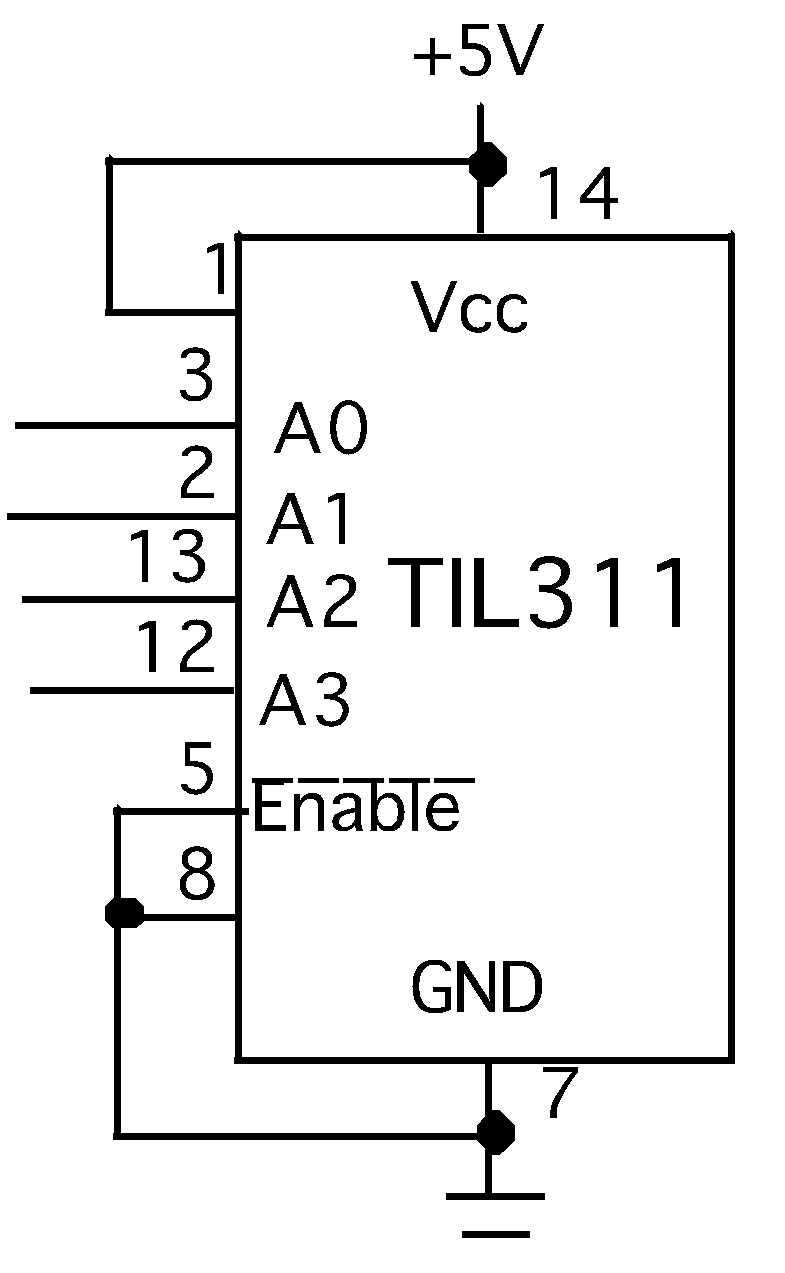
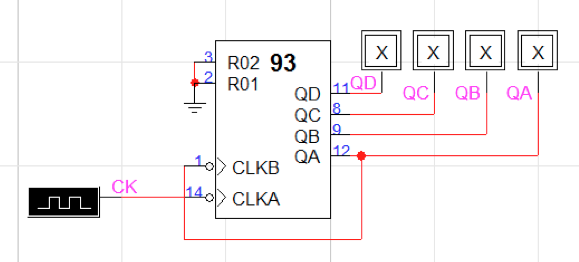
An IC 7493 is plugged into your workbench at the top right. Examine the following pinout and logic diagram, and the accompanying picture of wires in the board:
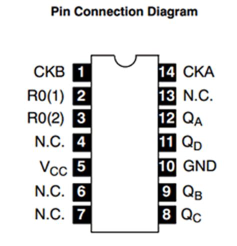
Which wire in the picture represents the Vcc connection?
Example answer: The short red wire connected to the third foot from the bottom on the left side of the chip.
Which wire in the picture represents the GND connection?
Example answer: The short black wire connected to the third foot from the bottom on the right side of the chip.
Which pin does the wire that leaves the edge of the picture connect to? Where is it going?
Example answer: It’s connected to the top-right pin. Since pins are counted counterclockwise around the chip from the top-left and there are 7 pins on each side, that’s pin #14. It’s going out-of-frame because it needs to connect to the push-button input all the way on the bottom-left side of the workbench.
Why are pins 8, 9, 11, and 12 connected to indicators numbered 6, 7, 5, and 8, instead of being connected to LEDs in the same order as the pins are listed?
Example answer: That’s because the logic diagram shows that outputs QA, QB, QC, and QD are connected on pints 12, 9, 8, and 11, i.e., NOT in increasing pin order. We want the LEDs to be in-order according to the output labels, not the pin numbers.
Now, go ahead and wire up the chip on your own board, as shown in the picture / according to the logic diagram. (Check the section on logic diagrams in the slides: you need to map the diagram to the actual physical layout of the chip.)
Turn the power on, and observe the four logic indicators. Press the PB1 button repeatedly, until all of them indicate low voltage.
Now continue pressing PB1, recording the logic indicator outputs (1 for on/high-voltage and 0 for off/low-voltage) in the table to the right until all of the indicators are off again (click on each cell to toggle between 0 and 1).
Do you recognize this pattern? Describe what the 7493 chip does concisely:
Example answer: It’s a 4-bit binary counter that counts up by 1 each time the button is pressed and then released.
Now turn off the power, but don’t disconnect the circuit.
GCorrect answer:
| Presses | QD | QC | QB | QA |
|---|---|---|---|---|
| 0 | 0 | 0 | 0 | 0 |
| 1 | 0 1 |
0 1 |
0 1 |
0 1 |
| 2 | 0 1 |
0 1 |
0 1 |
0 1 |
| 3 | 0 1 |
0 1 |
0 1 |
0 1 |
| 4 | 0 1 |
0 1 |
0 1 |
0 1 |
| 5 | 0 1 |
0 1 |
0 1 |
0 1 |
| 6 | 0 1 |
0 1 |
0 1 |
0 1 |
| 7 | 0 1 |
0 1 |
0 1 |
0 1 |
| 8 | 0 1 |
0 1 |
0 1 |
0 1 |
| 9 | 0 1 |
0 1 |
0 1 |
0 1 |
| 10 | 0 1 |
0 1 |
0 1 |
0 1 |
| 11 | 0 1 |
0 1 |
0 1 |
0 1 |
| 12 | 0 1 |
0 1 |
0 1 |
0 1 |
| 13 | 0 1 |
0 1 |
0 1 |
0 1 |
| 14 | 0 1 |
0 1 |
0 1 |
0 1 |
| 15 | 0 1 |
0 1 |
0 1 |
0 1 |
Correct answer: See above
Exercise 2: Hex Display
Below the 7493 chip on your board is a TIL311 chip. We’ll connect it to the outputs of the 7493 to see how it works.
Follow the logic diagram shown below to connect the TIL311, referring to the logic diagram of the 7493 that we’ve shown above as well, and to the pinout for the TIL311 also shown below. From the 7493 to the TIL311, You’ll need to connect QA to A0, QB to A1, QC to A2, and QD to A3. Then wire up the Vcc, GND, and enable inputs of the TIL311 so that it is activated. The picture on the right shows what this should look like when connected on your board:
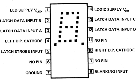
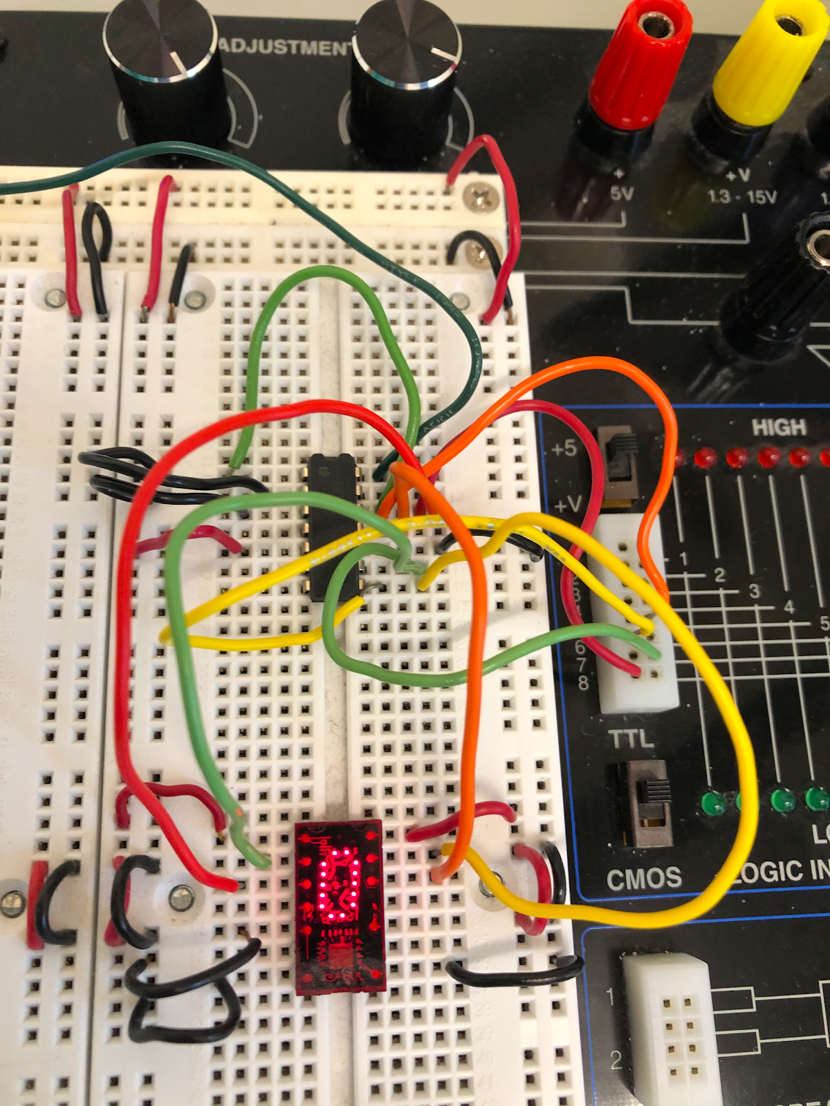
Once you have completed your wiring, power the board back on and record the symbols displayed on the TIL311:
- What symbol is displayed when the outputs of the 7493 are all 0? Correct answer: 0
- What symbol is displayed when the outputs of the 7493 are 0101? Correct answer: 5
- What symbol is displayed when the outputs of the 7493 are 1010? Correct answer: A
- What symbol is displayed when the outputs of the 7493 are 1111? Correct answer: F
What do these symbols represent? What is the purpose of the TIL311, and how is it related to what the 7493 does?
Example answer: These are the hexidecimal digits corresponding to the binary inputs, interpreted as a single integer value. The purpose of the TIL311 is to display a 4-digit binary number as a hex digit that humans can easily read. Since the 7493 counts clock pulses as a 4-wire binary signal, the TIL311 works well with it to take in 4 binary signals and display the corresponding number.
Exercise 3: Timing Diagrams
Using a simulator, you can create a timing diagram that shows patterns of high and low voltage over time. Although a truth table is sufficient to describe the behavior of a combinational circuit, for sequential circuits, a timing diagram is needed, since the outputs depend not only on the instantaneous state of the inputs, but on the history of activations over time.
Ti] learn more about LogicWorks and the Falstad simulator, we’ll hook up the same circuit you just built on the workbench in both simulators. Consult the diagrams and instructions below to hook things up:
To build these circuits, follow these directions:
LogicWorks
- Search for ‘74_93’ to create the 7493 chip.
- Note that the Vcc and ground connections are automatic.
- Search for ‘clock’ to make a clock component to use for input to CLKA.
- Connect R01 and R02 to ground (search “ground”).
- Search for “binary” and use “Binary Probe” to hook up the outputs (one probe attached to each ouptut).
- Drag a wire from the CLKB input around to the right-hand side and hook it up to the QA output (doing this in two steps is easiest, first dragging down and to the right, and then clicking again and dragging up).
- Use the Text tool (‘A’ symbol) to label the
connections to the clock and to each binary probe.
- Make sure the labels turn pink, which should happen when you hit the wire.
- These should show up in the timing window at the bottom as they are labeled.
- Once the circuit is complete, click “clear unknowns” (stomping foot
icon). Use the slider near the ‘stop’ button to slow down the simulation
speed.
- Use “clear unknowns” while the simulator is running.
Use the Simulation -> Show Values option to get LogicWorks to display the voltage state of each wire.
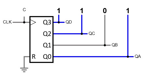
Falstad
- Use Draw -> Digital Chips -> Counter to create the counter
chip.
- Note the lack of R02 and CLKB. This is simpler than a 7493.
- Draw -> Inputs and Sources -> Clock for the clock input.
- Draw -> Inputs and Sources -> Ground for the ground connection.
- Draw -> Logic Gates, Input and Output -> Logic Output for the
indicators.
- Double-click and select “numeric;” then copy/paste
- Draw -> Outputs and Labels -> Labeled Node for the labels.
- To display the timing graph, right-click each label in order and
select “view in new scope.” Then select Scopes -> Stack All.
- The labels for each scope won’t be shown, but you can hover over them to see which label they correspond to.
You can use this simulator window to build the Falstad version of the circuit. You’ll have to open LogicWorks separately.
When you’ve built the circuit in both Falstad and LogicWorks, take a look at the signals shown in the timing window. They should match the patterns shown below:
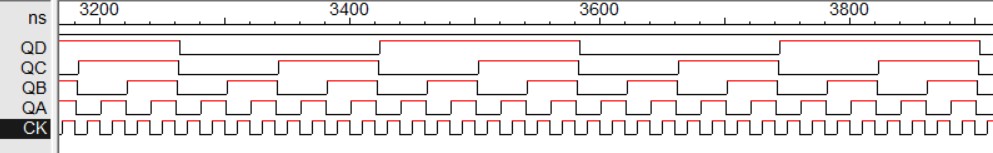
How long is each high-voltage-period of the QD signal relative to the high-voltage periods of the clock signal?
Example answer: 16 times as long.
Referring to the first diagram above, imagine that the bottom signal in that diagram (the clock signal which has the shortest pulses) is generated by pressing a button, with each high pulse happening while the button is held down and each low pulse when the button is released. In that scenario, do the QA-QD signals (the four above the clock signal) update when the button is pressed, or when it is released?
When it’s
pressed.
When
it’s released.
Now look at the second diagram above (the one without numbers along the top axis). In this diagram, the clock signal is the top one. Does it have the same behavior as the LogicWorks diagram you looked at for the previous question, in terms of when things update relative to the clock edges?
Yes, it
behaves the same.
No,
it’s different.
Explanation: The two
simulators do things differently: Falstad’s 7493 equivalent updates on
rising edges, while LogicWorks’ version updates on falling edges. We’ll
see more about edges in later labs.
Describe how the timing diagrams are related to the truth table for the binary counter:
Example answer: At each time point in the timing diagram, we can see whether each signal is low or high. In the truth table for binary numbers, the QA column flips between 0 and 1 in each row, then the QB flips every other row, the QC every 4 rows and QD every 8 rows. In the timing diagrams, we have the same relationship between signals and clock ticks: the QA signal flips from high to low on the down-tick of each clock pulse, QB flips every other clock pulse, QC every four pulses, and QD every 8.
Exercise 4: Circuit Design
A parity bit is an extra bit of information which is sent when data is transmitted, to check for errors in transmission.
For a given set of bits, the occurrences of bits whose value is 1 is counted. If that count is odd, the parity bit value is set to 1, making the total count of occurrences of 1’s in the whole set (including the parity bit) an even number. If the count of 1’s in a given set of bits is already even, the parity bit value is 0, so in that case the count remains even for the whole set.
Fill in the truth table at the right for P, to produce an even parity bit for inputs ABCD.
An XOR or “exclusive or” gate is useful in a circuit to produce a parity bit. Why?
Example answer: When combined with XOR, high bits will cancel each other out, but will persist when paired with a low bit. So for the 2 bits going into an XOR gate, the result of the XOR will be a 1 if there were an odd number of input bits turned on, and a 0 if there were an even number turned on.
Using either LogicWorks or the Falstad simulator (there’s a window below), design a circuit with 4 inputs whose output P is the parity bit for those four inputs, according to the truth table you just filled out. Use XOR gates. Describe your design:
Example
answer: The inputs are grouped into two pairs
and fed into two XOR gates. The outputs from these enter a third XOR
gate to produce the parity bit. 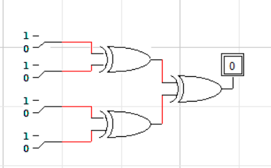
Test your design using 4-5 rows of the truth table you just completed.
GCorrect answer:
| A | B | C | D | P |
|---|---|---|---|---|
| 0 | 0 | 0 | 0 | 0 1 |
| 0 | 0 | 0 | 1 | 0 1 |
| 0 | 0 | 1 | 0 | 0 1 |
| 0 | 0 | 1 | 1 | 0 1 |
| 0 | 1 | 0 | 0 | 0 1 |
| 0 | 1 | 0 | 1 | 0 1 |
| 0 | 1 | 1 | 0 | 0 1 |
| 0 | 1 | 1 | 1 | 0 1 |
| 1 | 0 | 0 | 0 | 0 1 |
| 1 | 0 | 0 | 1 | 0 1 |
| 1 | 0 | 1 | 0 | 0 1 |
| 1 | 0 | 1 | 1 | 0 1 |
| 1 | 1 | 0 | 0 | 0 1 |
| 1 | 1 | 0 | 1 | 0 1 |
| 1 | 1 | 1 | 0 | 0 1 |
| 1 | 1 | 1 | 1 | 0 1 |
Correct answer: See above
Here’s a Falstad simulator window if you’d like to use it instead of LogicWorks:
Exercise 5: Bit Puzzles
On the next assignment, you will write some short C programs which implement functions using a limited set and number of C bitwise, logic, and arithmetic operations.
The functions you will write will perform some logical operation. You are given a skeleton for each function, and you will replace the “return” expression with one or more lines of C code that implements the function. Your code must conform to the following style:
int Funct(arg1, arg2, ...) {
    /* brief description of how your implementation works */
    int var1 = Expr1;
    ...
    int varM = ExprM;

    varJ = ExprJ;
    ...
    varN = ExprN;
    return ExprR;
}
Each “Expr” is an expression using ONLY the following:
- Integer constants 0 through 255 (0xFF), inclusive. You are not allowed to use big constants such as 0xffffffff.
- Function arguments and local variables (no global variables).
- Unary integer operations
!~ - Binary integer operations
&^|+<<>>
Some of the problems restrict the set of allowed operators even further.
Each “Expr” may consist of multiple operators. You are not restricted to one operator per line.
You are expressly forbidden to:
- Use any control constructs such as
if,do,while,for,switch, etc. - Define or use any macros.
- Define any additional functions in this file.
- Call any functions.
- Use any other operations, such as
&&,||,-, or?: - Use any form of casting.
- Use any data type other than
int. This implies that you cannot use arrays, structs, or unions.
You may assume that your machine:
- Uses 2s complement, 32-bit representations of integers.
- Performs right shifts arithmetically.
- Has unpredictable behavior when shifting an integer by more than 32 bits.
Note: Integers are represented as 32-bit values in our machines. But, it is cumbersome to write that many digits on paper when you are verifying your results by hand. So, pretend you only have 4-bit representation (it will usually translate to a correct solution for 32-bit numbers, as well).
Here is an example of the type of functions you will write:
/*
 * pow2plus1
 * returns 2ⁿ + 1, where 0 <= n <= 31
 */
int pow2plus1(int n) {
       return (1 << n) + 1;
}
Explain why shifting left is an important part of the solution:
Example answer: We’re not allowed to use a function like pow from math.c, and since n is a variable, without being able to use a loop, we can’t fall back on repeated multiplication to compute 2^n. However, shifting left multiplies by 2, so 2^n can be computed by using a left shift, which is the only option available to us for this problem.
For each of the following values for n, show that 2ⁿ + 1 is equivalent to (1 << n) + 1:
If you prefer, you can do your work on paper.
n = 0 = 0000₂
Example
answer: 2^0 + 1 is 1 + 1 or 2.
1
<< 0 is 1, and 1 + 1 is also 2.
n = 1 = 0001₂
Example
answer: 2^1 is 2, plus 1 is 3.
1
<< 1 is 10₂ which is 2 in base 10, plus 1 is 3.
n = 3 = 0011₂
Example answer: 2^3 is 8, plus 1 is 9. 1 << 3 is 1000₂, which is 8 in base 10, plus 1 is also 9.
Now, write a solution for the following function, using the specified rules:
/*
 *   bitOr(int x, int y)     produces    x | y    using only ~ and &
 *   Example: bitOr(6, 5) = 7
 *   Legal ops: ~ &
 *   Max ops: 8
 */
int bitOr(int x, int y) {
  return 2;     // 2 is just a placeholder; replace it
}/*
* bitOr(int x, int y) produces x | y using only ~ and &
* Example: bitOr(6, 5) = 7
* Legal ops: ~ &
* Max ops: 8
*/
int bitOr(int x, int y) {
return ~(~x&~y);
}Show that your code works by expressing the following values as 4-bit binary numbers and showing your work:
x = 1, y = 3
x = 0001₂ y = 0011₂
~x = 1110₂ ~y = 1100₂
~x & ~y = 1110₂ & 1100₂ = 1100₂
(x & ~y) = 0011₂ = 3
x|y = 0001₂|0011₂ = 0011₂ = 3
x = 0, y = 5
x = 0000₂ y = 0101₂
~x = 1111₂ ~y = 1010₂
~x & ~y = 1111₂ & 1010₂ = 1010₂
(x & ~y) = 0101₂ = 5
x|y = 0000₂|0101₂ = 0101₂ = 5
x = 3, y = 4
x = 0011₂ y = 0100₂
~x = 1100₂ ~y = 1011₂
~x & ~y = 1100₂ & 1011₂ = 1000₂
(x & ~y) = 0111₂ = 7
x|y = 0011₂|0100₂ = 0111₂ = 7
Given a positive integer, write a function to find if it is a power of two or not.
/*
 * isPower2 - returns 1 if x is a positive value which is power of 2, and
 *     returns 0 otherwise
 *   Examples: isPower2(5) = 0, isPower2(8) = 1, isPower(-1) = 0,
 *     isPower2(0) = 0
 *   Legal ops: ! ~ & ^ | + <<  >>
 *   Max ops: 20
 *   Rating: 4
 */
int isPower2(int x) {
  return 2;     // 2 is just a placeholder; replace it
}
If you were writing a program in Python or Java, how would you detect a power of 2?
First thing I can think of is to use modulus with 2 followed by division in a loop until we end up with either a 1 somewhere as a result of the modulus (so it’s not a power of 2) or the value ends up as 1:
def ip2(x):
    while x > 1:
        if x % 2 != 0:
            return False
        x //= 2
    return True
If you cannot apply this strategy in C using the rules given for this assignment, study some values to see if you recognize any patterns in the numbers which may help you.
Write down the 4-bit values for numbers 0 to 7:
GCorrect answer:
| Decimal | Binary |
|---|---|
| 0 | Correct answer: 0000 |
| 1 | Correct answer: 0001 |
| 2 | Correct answer: 0010 |
| 3 | Correct answer: 0011 |
| 4 | Correct answer: 0100 |
| 5 | Correct answer: 0101 |
| 6 | Correct answer: 0110 |
| 7 | Correct answer: 0111 |
Correct answer: See above
Which of these are powers of 2?
Example answer: 0001, 0010, 0100
Do you notice anything significant about the pattern of bits for the numbers that are powers of 2 compared to the other values?
Example answer: They’re the only patterns which include exactly 1. All other patterns have either 0 1’s or more than 1 1.
Experiment with how you can use the allowed operators to detect the powers of 2. You can use:
! logical NOT
~ bitwise complement
& bitwise AND ^ bitwise XOR
| bitwise OR + addition
You can also use constant values up to 255 (0xFF) in your expressions.
Because all numbers which are a power of two have only one bit position set, one less than a power of two will always have all the bits lower than that position set and all the bits above that 0.
Here are the powers of 2 with the next smaller number,
x + -1, below them:
| Expr | |||
|---|---|---|---|
x: |
0001 | 0010 | 0100 |
x-1: |
0000 | 0001 | 0011 |
Experiment with applying each of the allowed bitwise operators to the pairs of numbers x and x-1.
What operator gives you the same result for each pair?
Example
answer: & operator gives
0000 for each pair.
Now, for the non-powers of two x, list x + -1 and apply
the operator you discovered:
Non-powers of 2
GCorrect answer:
| Expr | ||||
|---|---|---|---|---|
x: |
0011 | 0101 | 0110 | 0111 |
x-1: |
0010 | 0100 | 0101 | 0110 |
| Correct answer: 0010 | Correct answer: 0100 | Correct answer: 0100 | Correct answer: 0110 |
Correct answer: See above
Do you get the same result by applying the operator to these pairs of values as you did for the powers of 2?
Example
answer: Nope, each of these gives a non-zero
result when & is applied.
If your answer is no, you have found a way to detect a power of 2!
Write an expression that returns 0 for non-powers of 2 (Note:
x-1 can be accomplished with x + ~0):
Example
answer: !(x & (x + ~0))
If x = 0, will you get the correct result with this expression?
Example
answer: No, because x + ~0 is 0000 + 1111,
which is 1111, and 0000 & 1111 is 0, so which when ! is
applied becomes 0001, which is wrong, because 0 is NOT a power of 2.
The answer should be no: so, the value 0 must be treated as a special case.
If the number is 0, you should simply return 0.
If the number is stored in x, what expression will return 0 when the number is 0?
Example answer: Just x…
One of the bitwise operators can be used to connect the two expressions so that when x is 0, return 0, otherwise, return the expression which detects a power of two.
Write the full expression:
My first attempt (does work…)
!(x & (x + ~0)) + ~!x + 1
Less complex second term using ^ to combine them:
!(x & (x + ~0)) ^ !x
Will this expression also return 0 for all negative numbers?
Example answer: Nope
If not, add to your expression to also detect a negative value:
This version uses x >> 31 to get just the sign bit
of x, and then uses ! to produce a 0 for negative numbers
(positive sign bit) and a 1 for positive numbers. By combining that
using &, we effectively force the result to be 0 for
all negative numbers, but leave the result as-is based on the rest of
the expression for positive numbers.
!(x & (x + ~0)) ^ !x & ! (x >> 31)