CS 240 Lab 3: Arithmetic Logic
Peter Mawhorter
How do Computers Work?
How do Computer Circuits Work?
When you press the power button, some wires in the computer are powered with +5V, based on the transistors, which implement a series of logic gates. The logic gates are organized into common units called “chips” or “integrated circuits” (ICs).
A clock creates cycles of high and low voltage, which creates patterns of activation over time determined by the chips. Buttons or other inputs may also create be woven into these patterns.
How do Computers Represent Things?
High/low voltage patterns in groups of wires represent numbers using binary. These numbers can also represent symbols via an encoding like ASCII.
Specialized chips create patterns of voltage from inputs to outputs which, when interpreted as binary, correspond to things like “counting” or “addition.”
But what about… ?
- Integrated circuits put together gates to perform various functions. Which circuits are used in a CPU, and what are their functions?
- How do the integrated circuits for basic binary operations like addition or multiplication work?
- How are clock signals generated & managed in the computer?
- How is memory implemented using gates?
- How can we change what a computer does by writing a program, instead of having to re-wire it?
How does the OS Work?
- When you boot the computer, it launches an operating
system, which provides things like graphical or text interfaces
for controlling the computer.
- Most computers have graphical interfaces and either a touch screen or a mouse, possibly in addition to a keyboard.
- Servers don’t have any direct inputs, but allow for remote connections, where input & output is via text.
- A text interface for controlling a computer is called a “shell” or “command line.”
How does the OS Work?
- Whatever interface you use, you will log in, and then proceed to
launch individual programs to do specific stuff, like browse the web or
edit a file.
- Programs are just another kind of file, and we can create new programs using things like text editors and compilers.
But what about… ?
- How does the “boot” process work? Where does the operating system actually start?
- What language does the “shell” use? Why are shells still around when we have graphical interfaces?
- How does one program launch another? How does the OS keep track of programs that are running? How do two programs run at the same time?
- How do compliers actually work? How does our text written in a programming language turn into a program, and what does a “program” actually consist of?

The schematic diagram of the full CPU.
The CPU connections listed as a table:
| Component | Inputs | Outputs |
|---|---|---|
| PC |
|
|
| Instruction Memory |
|
|
| Control Unit |
|
|
| Register File |
|
|
| Arithmetic Logic Unit (ALU) |
|
|
| Data Memory (RAM) |
|
|
| BEQ Logic |
|
|
Check-in
Self-directed learning:
- Shell
- C
- Putting the pieces together
Outline
Lab Projects
Project Details
- Details and example ideas
- Propose by lab 5 at the latest (short conversation in lab).
- Demo by lab 7 at the latest (short demo in lab).
- Can get help from tutors/instructors but not from each other.
Project Assessment
- Demo in lab (interactive conversation).
- Explain learning & effort, we will ask questions.
- We’ll recommend A-/A/A+ but you can negotiate.
- We could ask for specific extension/fix.
- Can self-assign up to B+ without a lab project.
Directing Signals
Multiplexer
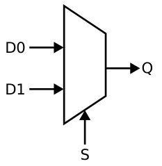
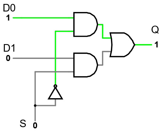
A multiplexer (or mux) selects one of inputs, using “select” wires whose activation pattern is interpreted as a binary number.
- An mux has input groups with wires each
- Each input group (& the output) has wires
- So an 8x2 mux has 16 inputs in 8 groups of 2, 3 select inputs, and 2 outputs.
2x1 Multiplexer
8x1 Multiplexer
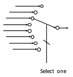
We can imagine that the select inputs change which input wire (or wire group) is connected to the output.
| S2 | S1 | S0 | Q |
|---|---|---|---|
| 0 | 0 | 0 | D0 |
| 0 | 0 | 1 | D1 |
| 0 | 1 | 0 | D2 |
| 0 | 1 | 1 | D3 |
| 1 | 0 | 0 | D4 |
| 1 | 0 | 1 | D5 |
| 1 | 1 | 0 | D6 |
| 1 | 1 | 1 | D7 |
D0-D8 are the Data inputs
Demultiplexer
A demultiplexer (or demux) is the inverse of a multiplexer: it steers an input value (or group) onto one of outputs based on select inputs.
- The unused output lines are low/0.
1x4 Demultiplexer
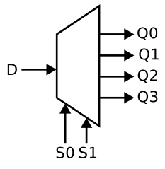
| S1 | S0 | Q3 | Q2 | Q1 | Q0 |
|---|---|---|---|---|---|
| 0 | 0 | 0 | 0 | 0 | D |
| 0 | 1 | 0 | 0 | D | 0 |
| 1 | 0 | 0 | D | 0 | 0 |
| 1 | 1 | D | 0 | 0 | 0 |
D is the data input
Untangling Binary
Decoder
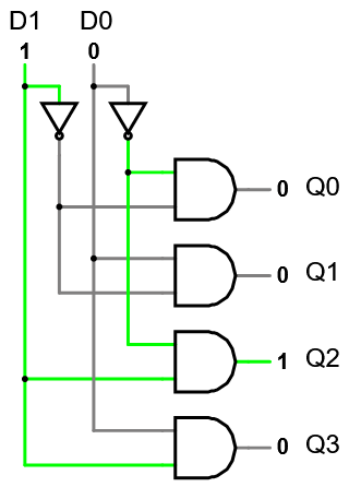
A decoder takes an -bit binary number on wires and outputs a high signal on one of wires with the rest low.
- Also known as a “1-hot” encoding where “hot” refers to high-voltage.
- Only one of the outputs is active at a time
- Numbers refer to inputs/outputs and is always equal to : you can have a 2x4 or 3x8 decoder, but a 3x5 decoder doesn’t make sense.
2x4 Decoder

3x8 Decoder Table
| D2 | D1 | D0 | Q7 | Q6 | Q5 | Q4 | Q3 | Q2 | Q1 | Q0 |
|---|---|---|---|---|---|---|---|---|---|---|
| 0 | 0 | 0 | 0 | 0 | 0 | 0 | 0 | 0 | 0 | 1 |
| 0 | 0 | 1 | 0 | 0 | 0 | 0 | 0 | 0 | 1 | 0 |
| 0 | 1 | 0 | 0 | 0 | 0 | 0 | 0 | 1 | 0 | 0 |
| 0 | 1 | 1 | 0 | 0 | 0 | 0 | 1 | 0 | 0 | 0 |
| 1 | 0 | 0 | 0 | 0 | 0 | 1 | 0 | 0 | 0 | 0 |
| 1 | 0 | 1 | 0 | 0 | 1 | 0 | 0 | 0 | 0 | 0 |
| 1 | 1 | 0 | 0 | 1 | 0 | 0 | 0 | 0 | 0 | 0 |
| 1 | 1 | 1 | 1 | 0 | 0 | 0 | 0 | 0 | 0 | 0 |
Encoder
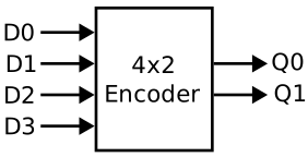
An encoder is the opposite of a decoder: it takes inputs where only one is on at once, and has outputs which encode the position of the input that was on in binary.
- Behavior is undefined if all inputs are off or more than one is on.
- Numbers refer to inputs/outputs and is always less than or equal to : you can have a 4x2 or 8x3 encoder, or even a 5x3 encoder, but you can’t have a 5x2 encoder (not enough bits of output).
4x2 Encoder
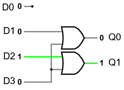
Note the disconnected input: when that’s the high input, neither output is on.
Addition
Half-Adder
A half-adder adds two one-bit values to get a 1-bit result, plus a 1-bit carry-out (which is 1 when both inputs are 1).
- Can’t use it for addition because it has no carry-in option
Full Adder
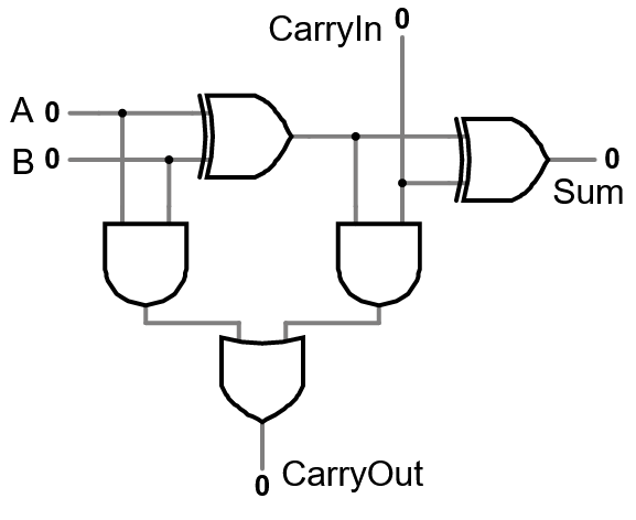
A full adder uses two half-adders to implement addition for 1 bit, with a carry-in and a carry-out.
- With 3 inputs, the max result is 11, which only needs 2 outputs.
- A “ripple-carry” adder for multiple bits hooks the carry-out from one adder into the carry-in of the next. This is how we add multi-bit numbers.