
🔬 Lab
CS 240 Lab 4
ALU & Sequential Logic
CS 240 Lab 4
In lab today, you will investigate the circuit which allows you to perform a variety of logical and arithmetic operations, the Arithmetic and Logic Unit (ALU), which is an essential part of a computer processor.
You will also investigate the behavior of several sequential logic circuits, which form the basis for the various kinds of memories needed to implement a computer.
Download this project file and use this link to open CircuitVerse. Use the project tabs specified below for each part of the lab.
Arithmetic Logic Unit
An Arithmetic Logic Unit (ALU) is a combinational circuit used to perform all the arithmetic and logical operations for a computer processor, and can be built using basic components that you are familiar with.
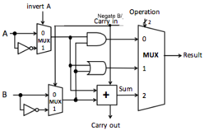
You saw a very simple ALU on the lab assignment. The circuit below also uses an additional set of 2x1 multiplexers at the inputs, controlled by new control lines “Invert A,” “Invert B, and it has a”Carry in” line.
“Invert A” allows you to invert the A input (for logical operations), and “Invert B” does the same for the B input.
“Carry in” allows you to add a carry-in bit to the adder, and when combined with “Invert B,” this lets you do subtraction, since (~B + 1) = -B, and thus A + (~B + 1) = A - B.
In the following circuit, the box with ‘+’ on it is a 1-bit adder. The “invert B” and “Carry in” inputs have been combined into one “Negate B / Carry-in” input. Assume Operation is a 2-bit value Op1 Op0, where Op1 is the 2s digit and Op0 is the 1s digit.
The basic operations are:
| Operation | Explanation |
|---|---|
| add | A + B + Carry in |
| sub | invert B = 1, Carry in = 1, then add |
| AND | A AND B |
| OR | A OR B |
| NOR | invert A=1, invert B=1, then AND |
| NAND | invert A=1, invert B=1, then OR |
The following partial truth table shows the inputs necessary to enact each of these operations. Note the clever use of DeMoragn’s law to get NAND and NOR operations. Also note that we can use one column for both “invert B” and “Carry in” because their values can be the same in every row.
| invert A | invert B/Carry in | Op1 | Op0 | Result |
|---|---|---|---|---|
| 0 | 0 | 0 | 0 | A AND B |
| 0 | 0 | 0 | 1 | A OR B |
| 0 | 0 | 1 | 0 | A + B |
| 0 | 1 | 1 | 0 | A – B |
| 1 | 1 | 0 | 0 | A NOR B |
| 1 | 1 | 0 | 1 | A NAND B |
Exercise 1:
Predict the results for the circuit shown above. The “invA” column shows the value of the “invert A” input, while “invB&Cin” shows the value of the “Negate B/Carry in” input. The answers to the first combination of inputs are shown; click in the Cout and Result columns to cycle through answers):
| A | B | invA | invB&Cin | Op1 | Op0 | Cout | Result | Check | Description |
|---|---|---|---|---|---|---|---|---|---|
| 0 | 0 | 0 | 0 | 0 | 0 | 0 | 0 | Result: 0 (0 AND 0) Cout: 0 (0 + 0 has no carry-out) |
|
| GCorrect answer: 0 | 1 | 0 | 0 | 0 | 1 | 0 1 |
0 1 |
Correct answer: See above | Example
answer: Result: 1 (0 OR 1) Cout: 0 (0 + 1 has no carry-out) |
| GCorrect answer: 0 | 1 | 0 | 0 | 0 | 0 | 0 1 |
0 1 |
Correct answer: See above | Example
answer: Result: 0 (0 AND 1) Cout: 0 (0 + 1 has no carry-out) |
| GCorrect answer: 1 | 1 | 0 | 0 | 1 | 0 | 0 1 |
0 1 |
Correct answer: See above | Example
answer: Result: 0 (1 + 1) Cout: 1 (1 + 1 has carry-out) |
| GCorrect answer: 0 | 1 | 0 | 1 | 1 | 0 | 0 1 |
0 1 |
Correct answer: See above | Example
answer: Result: 1 (0 + 0 w/ carry-in) Cout: 0 (0 + 0 + carry-in has no carry-out) |
| GCorrect answer: 1 | 1 | 0 | 0 | 0 | 0 | 0 1 |
0 1 |
Correct answer: See above | Example
answer: Result: 1 (1 AND 1) Cout: 1 (1 + 1 has carry-out, even though that’s not the operation we care about) |
| GCorrect answer: 1 | 1 | 1 | 1 | 0 | 0 | 0 1 |
0 1 |
Correct answer: See above | Example
answer: Result: 0 (0 AND 0 since A and B are inverted) Cout: 0 (0 + 0 + carry-in has no carry-out) |
Select the “ALU Parts” tab of the Circuitverse project linked at the start of the lab.
Build a 1-bit ALU by connecting the provided parts together.
Check your connections against the “1-bit ALU” tab if you get stuck.
Verify your predicted results by running thorough the test cases in the “1-bit ALU Test” tab as follows:
- The testers should already be hooked up for both your version and
the solution circuit. The “Inputs” row should display
0043while the “Result” and “Expected” rows should show0002, and therefore “Errors” should be0000.If you see different values, click on the gray circle (button) connected to the “RST” input to reset both testers. If you still see different values, you’ll need to reset the “EEPROM” data for both testers. To do that, select the EEPROM, then choose “Load Data” from the “Properties” panel, and paste in the following text:
0x00020043 0x00030047 0x00030003 0x00000001 0x00000002
0x00010022 0x00010021 0x00000029 0x00000032 0x00020057
0x00030023 0x00030026 0x00000000
- Click the “CLK” button to move to the next test. If the “Wrong” light comes on, that test failed for your circuit (or the solution, if the light comes on for the solution tester). When “Wrong” comes on, “Failed” will come on too and stay on until the next reset.
- Keep clicking the “CLK” button until either a test fails or you get to the point where the same test repeats again and again.
Click here if you want to understand the test setup in more detail.
The test setup here is complicated, with 8 hex digits in each test, 4 of which are the expected result and 4 of which are the test inputs (but only 7 of those 16 input bits and 2 of the 16 result bits are actually used). You can convert the last two digits shown on the “Input” row to binary and look at the right-hand 7 of those 8 bits to determine what the 7 inputs are for each test. Similarly, the “Expected” and “Result” rows in binary specify the expectations & results for the “Result” and “Carry-out” bits of the ALU.
Look at the breakout/splitter in the test circuit to see which bits of the input hex digits are used for which inputs of the ALU: it starts with bit 0 (the least-significant bit) feeding into the “A” input.
Reminder: A breakout (or “splitter”) takes a bundle of wires and splits it up into single wires and/or smaller bundles. Each smaller bundle is labeled with a number (or two numbers separated by a colon) to indicate which wires it includes. In the “1-bit ALU Test” circuit we have a breakout that splits off wires 0, 1, 2, 3, 4, and 5:6. This splits the first 7 wires from the 16 test inputs, and directs wire 0 to input A, wire 1 to B, 2 to Carry-in, etc. In this case, since the “Opcode” input needs 2 wires, wires 5 and 6 are sent there together.
If we use have 0043 as the input digits and
0002 as the expected digits (both in hexadecimal)…
What inputs are being sent to the chip being tested?
- A: 0
1 - B: 0
1 - Carry-in: 0
1 - Invert A: 0
1 - Invert B: 0
1 - Opcode: 00
01
10
11
- A: 0
What values are expected for the result and carry-out?
- Result: 0
1 - Carry-out: 0
1
- Result: 0
What operation does this correspond to, and why?
Example answer: 1 + 1 = 0 with carry-out. The hex digit
4specifies bits 4-7 of the inputs, but since there are only 7 input bits needed, bits 0-2 of those 4 are used as the “Invert B” and “Opcode” values. A 4 is0100in binary, so we’re setting the Opcode to 10 and the “Invert B” to 0. The hex digit3is specifying the “Invert A”, “Carry-in”, “B”, and “A” digits in that order from left to right, and in binary it’s0011, so we are setting A = 1 and B = 1, while leaving Carry-in and “Invert A” as zeroes. We’d expect 1 + 1 to result in a 0 with carry-out, so the expected bits are10or 2 in hexadecimal.
If a test is failing and you’re not sure why, ask your instructor for help.
Exercise 2:
It is possible to make a 4-bit ALU by connecting four 1-bit ALUs together in a similar way to how you connected 4 1-bit adders to make a 4-bit adder in lab last week (assuming you got to the stretch exercises). The “4-bit ALU” tab in CircuitVerse has everything already hooked up for a 4-bit ALU, minus some extra outputs that we’ll have you build in a bit.
For now, without testing the 4-bit ALU in the simulator but just based on your knowledge of how a 4-bit ALU should work, predict the results in the table below, taking into account:
- A and B are 4-bit values represented by hex digits, and are signed two’s complement representations. Use this hex reference to help you translate between hex, binary, and decimal.
- When inverting B, a carry-in is also added automatically (this does not happen when inverting A).
- The Result is a 4-bit signed value and should be written as a hex digit.
- Cout, Sign, and Overflow are single bits.
- Cout and Overflow are produced according to the addition operator, even when the circuit is performing a different operation.
The definitions for each column are:
- Result is the result for the selected operation.
- Cout is the carry-out bit from addition. This is always computed by the adder, whether or not the operation is addition.
- Sign is the sign bit of the result (the most-significant bit).
- Overflow is true if there’s overflow from the adder (assuming signed two’s-complement numbers). Overflow is always computed by the adder, whether or not the operation is addition.
- Zero should be true if and only if the result is exactly 0.
| Function | Test Inputs | Result (in hex) |
Cout | Sign | Overflow | Zero | Check |
|---|---|---|---|---|---|---|---|
| A PLUS B | A=3, B=7 | A | 0 | 1 | 1 | 0 | |
| GCorrect answer: A PLUS B | A=F, B=E | Correct answer: D | 0 1 |
0 1 |
0 1 |
0 1 |
Correct answer: See above |
| GCorrect answer: A AND B | A=1, B=F | Correct answer: 1 | 0 1 |
0 1 |
0 1 |
0 1 |
Correct answer: See above |
| GCorrect answer: A AND B | A=7, B=8 | Correct answer: 0 | 0 1 |
0 1 |
0 1 |
0 1 |
Correct answer: See above |
| GCorrect answer: A OR B | A=3, B=C | Correct answer: F | 0 1 |
0 1 |
0 1 |
0 1 |
Correct answer: See above |
| GCorrect answer: A MINUS B | A=3, B=4 | Correct answer: F | 0 1 |
0 1 |
0 1 |
0 1 |
Correct answer: See above |
Exercise 3:
Given the simulated 4-bit ALU in CircuitVerse, describe the underlying connections/logic needed to produce the Sign, Overflow, and Zero outputs (including any gates that are required).
Sign bit:
Example answer: The sign bit is wired to the most-significant bit of the 4 output lines, which is the sign bit in two’s-complement arithmetic.
Overflow bit:
Example answer: The more complex way is to do (NOT(A3 XOR B3)) AND (A3 XOR R3). This breaks down into NOT(A3 XOR B3) which is true when A3 is the same as B3, along with A3 XOR R3 which is true when A3 is different from R3. In other words: “Signs were the same going in, but we got the opposite sign coming out.” An easier way to implement this is to just XOR the carry-in and carry-out for the last 1-bit ALU. That works because if there’s carry-in, there will be carry-out unless both sign bits are 0, in which case there must be overflow since we had two zeroes going in but a carry means a 1 will go out. On the other hand, if there’s no carry-in, there can only be carry-out if both sign bits were 1’s, meaning we added two negative numbers and due to carry-out ended up with a positive number.
Zero bit:
Example answer: The Zero bit is wired to the result of a 4-input NOR gate (or several 2-input OR gates with a NOT gate at the end to emulate a 4-input NOR) that takes all 4 bits of output as its inputs. That way, the Zero bit is 1 when the value of the output is exactly 0000₂, and 0 otherwise.
Exercise 4:
Now add the gates you just described to the “4-bit ALU” tab in CircuitVerse, using the provided Sign, Zero, and Overflow outputs.
Verify that your outputs work by running through the test cases in the “4-bit ALU Test” tab (you can check your designs against the “4-bit ALU extras” solution).
The first test (after clicking the reset button) should show
0273 as the inputs. If it doesn’t show that, load the
following data into the EEPROM:
0x00aa0273
0x003d02ef
0x001100F1
0x00400087
0x002f01c3
0x00500c96
0x002f0a43
0x00130a9c
0x00a90245
0x00400000
0x00400000
0x00400000
0x00400000
0x00400000
0x00400000
0x00400000
0x00400000
Ask your instructor for help if any of the test cases fail and you can’t figure out why.
SR Latch
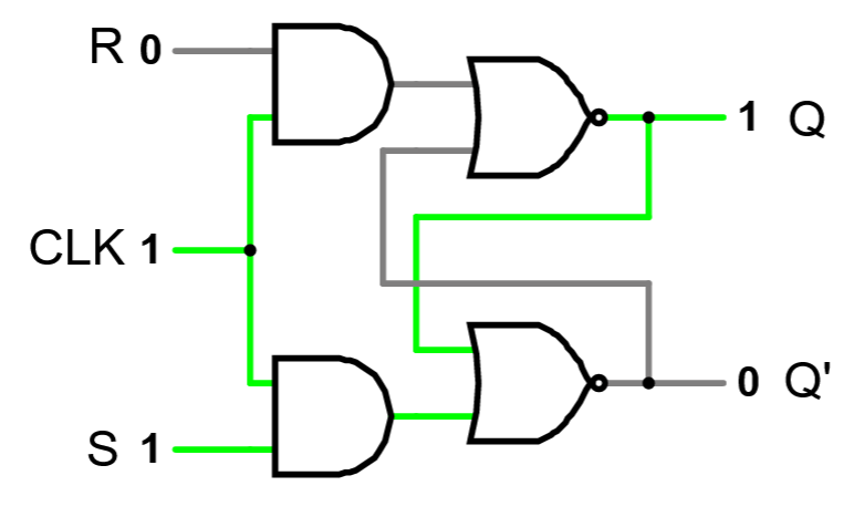
The SR latch is the basic unit of memory in most modern computers:
S means set the output to 1, and R means reset the output to 0. The two outputs Q and Q’ should always be opposites of each other.
Qp is the previous state of the latch. If you neither set or reset the circuit, it remembers its previous state. This means it is a bistable circuit: it has two stable voltage configurations, and external input can force it to swap between them.
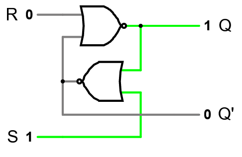
| S | R | Q | Q’ |
|---|---|---|---|
| 0 | 0 | Qp | Qp’ |
| 0 | 1 | 0 | 1 |
| 1 | 0 | 1 | 0 |
| 1 | 1 | 0 | 0 |
Exercise 5:
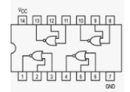
Build this circuit on your workbench, using:
- 1 7402 NOR chip (inserted at top right)
- two logic switches as inputs to S and R
- two logic indicators as outputs Q and Q’
Here is the pinout for the 7402:
First, plan out how you will connect the circuit, by filling in the following table:
| Purpose | Comes from | Connect to | Check row |
|---|---|---|---|
| R input | logic switch | pin 2 | N/A |
| Voltage supply | GCorrect answer: … pin 1 pin 7 pin 8 pin 14 |
Voltage supply on board | Correct answer: See above |
| Ground | GCorrect answer: … pin 1 pin 7 pin 8 pin 14 |
Ground on board | Correct answer: See above |
| Q output | GCorrect answer: … pin 1 pin 2 pin 3 pin 4 |
pin 5 and … logic indicator pin 3 pin 4 pin 6 |
Correct answer: See above |
| S input | GCorrect answer: … pin 1 logic switch pin 4 |
… pin 3 pin 4 pin 6 |
Correct answer: See above |
| Q’ output | GCorrect answer: … pin 1 pin 2 pin 3 pin 4 |
… pin 3 pin 4 pin 5 and logic indicator |
Correct answer: See above |
Verify the circuit by following these steps:
Set S=1 and R=0. What is Q? 0
1Now set S=0 and R=0. What is Q? 0
1Now set R=1, leaving S=0. What is Q? 0
1Set R back to 0, leaving S=0. What is Q? 0
1Why doesn’t Q return to 1, the value it had last time S=0 and R=0?
Example answer: Since the most recent value was Q=0, and we’ve only turned off inputs since then, without a reason to swap to the other stable configuration, the circuit stays in the one it’s in, where Q=0.
Now set both S=1 and R=1. What happens to Q and Q’?
Example answer: They’re both set to 0, since both NOR gates have an active input. This violates the design principle that they should be opposites.
Now set S=0 and R=0, and turn off the board, then turn it back on. What is the value of Q? Explain why the answer to that question is complicated:
Example answer: Since the board was powered off, the remembered value gets cleared out (all wires return to neutral voltage). When you power it on, neither NOR gate has high-voltage inputs, since R=0 and S=0, and the feed-back connection isn’t high-voltage to start with. Both gates will try to activate simultaneously, since NOR logic dictates their output should be high if both inputs are off. This sends power to one input of both gates, and so they then both try to deactivate, restarting the cycle. Practically, one of them will be slightly faster to activate eventually, preventing the other gate’s signal from flipping and thus stabilizing the circuit. But we can’t easily predict which one it will be, since it might depend on factors like precise manufacturing details of the chip, temperature of the two specific gates used in the chip, humidity, etc.
Don’t disconnect your circuit! You use it in the next exercise.
D Latch and Flip-Flop
The SR latch should only ever receive inputs 00, 10, and 01. 11 is problematic because it sets both Q and Q’ to 0, and because if we transition from 11 to 00, the outcome is unpredictable. The D latch makes a 11 input to the latch portion impossible, by using a single D input instead of S and R inputs, along with a clock. Here’s a circuit diagram for a D latch:
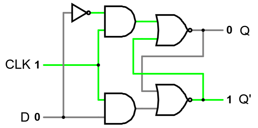
Note: The “CLK” input above is not an actual clock element, it’s just a logic input labeled “CLK.” We do this so that we can have manual control over when the clock shifts, instead of having to work around a constantly changing real clock.
Exercise 6:
Implement the clocked D latch circuit in CircuitVerse using the “D Latch (blank)” tab. Make sure to label your inputs “Clock” and “D” and your outputs “Q” and “Q’”.
When you first connect the circuit, it will be in an unpredictable state. Pulse the clock once to achieve valid inputs.
Verify your circuit by following these steps:
- Set D to 0, and CLK to 1; then set CLK back to 0. What is the value
of Q? 0
1 - Set D to 1. Does Q change? no
yes - Set CLK to 1. What is the value of Q? 0
1 - Now set CLK back to 0. Does the value of Q change? no
yes
What inputs should be used to set or reset the output, and what inputs can be used to remember the previous output?
Example answer: When you turn the clock on, set D to 1 to set the output, and set D to 0 to reset the output. Turning the clock off remembers the most recent setting, even when D changes.
Explain why this circuit solves the problem of S=R=1:
Example answer: The D input is sent to each AND gate but one of the lines is inverted, so it can ONLY send the equivalent of S=1/R=0 or S=0/R=1. This isn’t useful without the clock mechanism, as it wouldn’t be able to send S=0/R=0, but when the CK input is off, the latch gets S=0/R=0 and remembers the most recent state.
Exercise 7:
A D latch will change its state each time D changes, as long as the clock remains on. However, it would be even better to have a circuit which can “observe” D only for an instant, and then remember it the rest of the time. This is called a D flip-flop, and it changes its state only at the falling edge of the clock, remembering that observed state at all other times.
Next, construct a D flip-flop with a falling-edge trigger using the “D flip-flop parts” tab in CircuitVerse. You can check the “D Flip-Flop” tab for a solution if you get stuck.
Use the timing window in CircuitVerse to observe the behavior of the circuit over time, and answer these questions:
Toggle the D input off, and wait until Q2 becomes 0.
Try to quickly toggle the D input on and then off in such a way that the Q1 input never changes. When is this possible? Example answer: When the clock input is low, toggling the D input does not affect Q1 or Q2, so if you toggle D on and then back off before the clock input turns on again, Q1 will not change.
Now try to quickly toggle the D input on and then off so that Q1 changes to a 1 and then back to a 0, without ever changing Q2. When is this possible? Example answer: When the clock input is high, D directly affects Q1, but Q1 does NOT affect Q2. So during the on phase of the clock, you can toggle D1 on and then back off, which will also toggle Q1 for the same duration, but Q2 will not be affected.
Now turn D on and keep it there. When does the Q2 output change, relative to the clock signal? Example answer: It changes on the next falling edge of the clock that occurs after the D signal becomes a 1.
Now wait until the clock signal is low, turn D off again, and observe Q2. When does Q2 turn off?
Immediately.
As soon as the clock turns on again.
As soon as Q1 turns on.
The next time the clock turns off after being on again.When you toggled D while the clock input was low, Q1 didn’t change immediately (its clock signal was preventing that). But when the clock came on again, Q1 changed to match D. Why didn’t Q2 change as well at that point? Example answer: Q2 gets the opposite clock signal from Q1, so although the clock coming on allowed Q1 to match D, it also prevented Q2 from changing. Explanation: The time it takes for current to settle down across the NOT gate is short enough that the output Q1 won’t have changed by the time the clock signal is cut off from the second D latch. Only when the clock signal falls low again does the second D latch get its clock signal activated and finally update to match Q1, which had already changed to match D at the start of the clock tick.
This circuit remembers input, but only observes that input when the clock signal changes from high to low. This means that it can simultaneously receive input for a new state, while sending output from its old state, and flip over from the old to the new in an instant. Try the following:
- Disconnect the input switch from the D input (click on the wire coming out of it and hit ‘delete’).
- Take the output Q2 and connect it to a NOT gate oriented back towards the start of the circuit (after inserting the NOT gate, use the “Properties” panel to set the “Direction” to “LEFT”).
- Connect the output of that NOT gate back to the D input of the first D latch, where you just disconnected the input switch.
Notice: if this were a D latch, by connecting the output back to the input via a NOT gate, you’d have an inconsistent circuit: as soon as you turned the clock on, the circuit would rapidly flip back and forth between on and off, and it would be difficult to predict the state it would end up in when you turned off the clock. However, this circuit is different. Describe what happens if you connect the output Q2 through a NOT gate back to the input D:
Example answer: At each falling edge of the clock, the Q2 value changes to match the Q1 value, which has been storing the D input. This in turn flips the D input to the opposite of what it had been via the NOT gate. However, this does not create a contradiction, since with the clock off, the new D input does not affect Q1. At the next rising edge of the clock, the new D input gets forwarded to Q1, but still does not affect Q2, so the circuit is still consistent. Finally, at the second falling edge of the clock, the new Q1 value forwards to Q2, swapping the D input once more, and the cycle begins again. This circuit ends up creating an on/off pattern that consists of on pulses which are twice as long as the clock pulses it receives, always starting and ending on the falling edges of the input clock signal.
Register
A register is an n-bit memory (contains n flip-flops, which share a common clock, and are therefore all written to simultaneously). For example, the following diagram is an abstraction for a device that internally contains 16 D flip-flops, and can store 16 bits of information.
Note: the diagonal slash through a line indicates that the line represents multiple wires; for this example, 16. This is called a “bus” and when we separate the individual wires out of a bus, that’s called a “breakout,” or “splitter” in CircuitVerse terminology. To create a splitter in CircuitVerse, select it from the “misc” section of the “Circuit Elements” panel, and then you’ll be prompted for two inputs. At the first prompt, enter the total number of wires in the bus being split up (e.g., 16) and in the second prompt, enter several numbers with spaces between them that add up to the total you entered in the first prompt (e.g., if you enter “8 4 4” after putting “16” for the first prompt, you’ll get a splitter that splits a 16-wire bus into an 8-wire bus and two 4-wire buses.
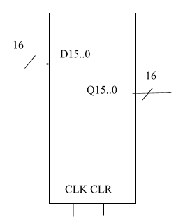
You can do the following with this device:
- You can read the current contents of the register at the outputs Q15..0
- You can write a new value to all 16 bits at once by setting the value at the inputs D15..0, and then pulsing (setting to high, then back to low) the CLK input.
- You can also clear all 16 bits to 0 at any time by activating the CLR input (when not using the CLR input, keep it set to 0).
Exercise 8:
For this exercise, use the “Register” tab in the CircuitVerse project.
Set the “Data in” to 0000000000001010. Make sure that
“Reset” is 0, and turn “Write” on and then off again. The “Data out”
output should match the input you just put in, and the hex digit
displays that show the 16 bit output & input in groups of 4 bits
should read 000A.
Now change the input data to 0000000000001111. Why does
the output data still show 000A?
Example answer: The register stores data, and only updates when the clock input falls. So although the inputs have changed, the stored data matches what was recorded when the “Write” input went from high to low.
Now, manipulate the circuit so that the output shows the hex digits
C5F0, and describe how you did that:
Example
answer: First, set the inputs to
C, 5, F, and 0,
which in binary becomes 1100, 0101,
1111, and 0000. Next, turn the clock on and
off again, to trigger an update of the stored
value.
Register File
A register file is a set of registers that can be read from and written to. We number the registers in the set, and use the numbers to specify which registers from the set are accessed at any particular time.
The register file in the “Register File” tab in CircuitVerse has 4 registers numbered 0, 1, 2, and 3, with “registers” 0 and 1 actually holding fixed values (0 for register 0 and 1 for register 1).
Each register stores 16 bits of data (similar to the register from the previous exercise).
Below is an abstraction for a register file with 16 registers instead of just 4. You can read the data from each of 2 registers and write new data to a third register simultaneously.
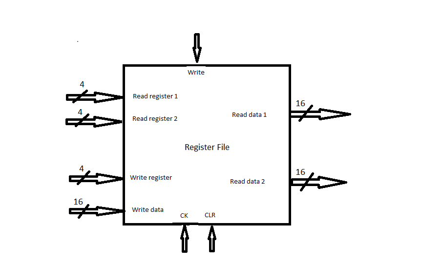
To read the contents of 2 registers at any given time, specify the number of the first register at the Read register 1 input, and the number of the second register on Read register 2.
The contents of the two registers are then available at the Read data 1 and Read data 2 outputs.
To write a new value to a specified register, set the Write register”” input to the number of the register, set the Write data** inputs to the value to be written to the register, set the Write input to 1, and then toggle the Clock input on and off again.
Exercise 9:
Open the “Register File” tab in CircuitVerse.
Toggle the “Reset” input on and off, which should set both registers back to all zeroes. Note that this register file has four “registers” but two of them are actually constant values, implemented by just connecting bundles of 16 wires to a combination of +5V and ground.
To write values into the two writeable registers, follow these steps:
- Set “Write Reg” to the binary number corresponding to the register you want to write to. In this circuit, registers 0 and 1 are constants, and registers 2 and 3 are writeable.
- Set “Write Data” to the value you want to write into the register you selected in step 1.
- Set “Write” to 1 (and ensure that “Reset” is 0).
- Toggle “Clock” on and then off again. The register value should update when you toggle it off.
Use this procedure to write ‘5EA1’ into register 2 and ‘F00D’ into register 3.
The register file supports reading stored data from two registers at once, but it can only write to one register at a time. Thinking about common operations that you use when programming, why might it be set up this way?
Example answer: Most basic operations like ‘+’ or ‘and’ or ’*’ need two values to operate on and produce a single result. So being able to read two values at once and store one result makes sense.
To read the values currently stored in the registers just set the “Read Reg 1” and “Read Reg 2” inputs to the binary numbers corresponding to the registers you want to read. The outputs will be displayed as “Read Data 1” and “Read Data 2” and will also show up in the hex displays on the right.
Write the value stored in each register from the table below. (Write values as upper-case 4-digit hex numbers, without any prefix). Remember you can read two at a time.
Set “Read Reg 1” to 00 and “Read Reg 2” to
01. What values are the outputs set to (answer with just
the hex digits displayed)?
GCorrect answer:
- Read Data 1: Correct answer: 0000
- Read Data 2: Correct answer: 0001
Correct answer: See above
Now set both “Read Reg 1” and “Read Reg 2” to 11. What
values are the outputs set to?
GCorrect answer:
- Read Data 1: Correct answer: F00D
- Read Data 2: Correct answer: F00D
Correct answer: See above
What values should you set “Read Reg 1” and “Read Reg 2” to so that
the outputs read 0000 for “Read Data 1” and
5EA1 for “Read Data 2”?
GCorrect answer:
- Binary value for “Read Reg 1”: Correct answer: 00
- Binary value for “Read Reg 2”: Correct answer: 10
Correct answer: See above
Stretch Exercises
Exercise 10:
Looking at the “Register File” tab in the CircuitVerse project, answer the following questions:
What is the purpose of the decoder chip in this circuit (the trapezoid on the left-hand side)?
Example answer: It turns a binary number specifying which register to write into a 1-hot encoding so that the clock for the indicated register can be turned on when the Clock input is on, while leaving the clock inputs for all other registers off.
If instead of using a decoder to ensure that only one of the internal registers gets a “Write” input, we used a demultiplexer to “send” the “Write data” input to just one of the registers while letting them all get a “Write” signal, what would happen?
Example answer: A demultiplexer “sends” data to one of N outputs by making that output get a copy of the data coming in, but it sends zeroes to all the other outputs that are not selected. So if you toggled the write input on all registers but only fed the data to one of them, this would get the data where it needs to go, but would reset all other registers to zeroes.
Does the “Clock” input need to be on/off/toggled in order to read data from the register file? Why or why not?
Example answer: Reading data from the register file happens automatically: as soon as the read register inputs are changed, the outputs change to reflect the value stored in that register, and the clock input is irrelevant to that process. The clock input is only needed to determine when a new value will be written into a register when “Write” is set to 1.
Extra Exercises
Exercise 11: Arithmetic Cycle
The register file has 2 data outputs and one data input. The ALU has two data inputs and one data output. Both have a few extra inputs to control things like which operation the ALU performs or where data is read from or written to in the register file.
If we hook up the ALU and register file to each other, so that data is read from the register file, processed in the ALU, and then written back to the register file, we’ve basically got a computer, which can perform a number of basic operations and store their results for further processing in subsequent steps. All we need to add to that is some way of specifying which operations to do on what data in what order.
The “Arithmetic Cycle” tab of the CircuitVerse project contains a 16-bit register file (with 4 registers) along with a 16-bit ALU. The inputs to the register file have already been connected, except for “Write Data.” The pre-specified settings provide 2 variable bits to specify one register to read from, but force reading from register 3 on the other data output, plus writing to register 3 when data comes in. The circuit also has a 5-bit “Operation” input.
Make the following connections to complete the design:
- Connect the data read from the two registers to the A and B inputs of the ALU.
- Connect the 5 “Operation” bits to the “Opcode”, “Invert A”, “Invert
B”, and “Carry in” inputs of the ALU. Use bits 0-1 for the opcode, bit 2
for “Invert A,” bit 3 for “Invert B,” and bit 4 for “Carry In.”
- You’ll need to use a custom “Splitter” for this from the “Misc” section of the “Circuit Elements” panel. Enter 5 for the first prompt (total number of bundled wires) and then “2 1 1 1” for the second prompt (split into 1 group of 2 and 3 groups of 1).
- Connect the ALU result to the “Write Data” input of the register file, so that the result gets stored back into register 3.
You can check your connections against the “Arithmetic Cycle (solution)” tab.
Once your connections have been made, do the following:
- Press the button connected to the “Reset” input of the register file to reset everything.
- Set the “Register A” input to
01and the “Operation” to00010. What operation will the ALU perform? Example answer: Because the opcode bits are10, it will do addition. The operands are0001(from the constant register 1) and0000(from register 3), so the result will be0001. - Press the button connected to the “Clock” input on the register file
to save that result. What digits are displayed on the hex displays at
the right? Correct
answer: 0002 Explanation: Because we just did 0 + 1 = 1 and stored a 1 in
register 3, the ALU now sees 1 + 1 = 2 and so the ALU result has
changed. However, this new result hasn’t yet been written into the
register file: we just wrote the old result of
0001there. - Press the clock button again. What is the value of register 3 at this point? Correct answer: 0002 Explanation: Now register 3 has actually been updated and holds a 2. This is displayed in the bottom row of the register file, since that’s the register we’re always reading from for “Read Data 2.”
By manipulating the “Operation” and/or “Register A” inputs, In less than 20 presses of the clock button, put a value into register 3 that has a digit other than 0 in the 3rd and/or 4th places from the right. What sequence of operations did you use to achieve this? Can you do it in a single clock press?
Example
answer: There are multiple ways of doing
this. One simple option is to subtract 1 from 0 to get
0xFFFF; this can be accomplished after a reset by setting
the register to 01 and the operation to 10110.
That operation value uses 10 as the opcode for “add”, but
sets “invert A” and “carry in” to perform B + ~A + 1 which
is the same as doing B - A. Another option is to add 1 to
register 3, and then set the “Register A” value to 11 while
leaving the operation bits as 00010 for normal addition. At
that point, since each clock press is doing B + B, you
double the value each time and can get up to 100 in 9 clock
presses from a reset, counting the initial press needed to add the
constant register 1 into register 3. You could also use a different
operator like OR in combination with an inverted
0.
Exercise 12:
If you’ve got the time, here are some extra tricky ALU exercises, similar to Exercise 2. As a reminder:
- A and B are 4-bit values represented by hex digits, and are signed two’s complement representations. Use this hex reference to help you translate between hex, binary, and decimal.
- When inverting B, a carry-in is also added automatically (this does not happen when inverting A).
- The Result is a 4-bit signed value and should be written as a hex digit.
- Cout, Sign, and Overflow are single bits.
- Cout and Overflow are produced according to the addition operator, even when the circuit is performing a different operation.
The definitions for each column are:
- Result is the result for the selected operation.
- Cout is the carry-out bit from addition. This is always computed by the adder, whether or not the operation is addition.
- Sign is the sign bit of the result (the most-significant bit).
- Overflow is true if there’s overflow from the adder (assuming signed two’s-complement numbers). Overflow is always computed by the adder, whether or not the operation is addition.
- Zero should be true if and only if the result is exactly 0.
| Function | Test Inputs | Result (in hex) |
Cout | Sign | Overflow | Zero | Check |
|---|---|---|---|---|---|---|---|
| GCorrect answer: A AND B | A=3, B=C | Correct answer: 0 | 0 1 |
0 1 |
0 1 |
0 1 |
Correct answer: See above |
| GCorrect answer: A OR B | A=3, B=C | Correct answer: F | 0 1 |
0 1 |
0 1 |
0 1 |
Correct answer: See above |
| GCorrect answer: A NOR B | A=6, B=9 | Correct answer: 0 | 0 1 |
0 1 |
0 1 |
0 1 |
Correct answer: See above |
| GCorrect answer: A MINUS B | A=C, B=9 | Correct answer: 3 | 0 1 |
0 1 |
0 1 |
0 1 |
Correct answer: See above |
| GCorrect answer: A PLUS B | A=5, B=4 | Correct answer: 9 | 0 1 |
0 1 |
0 1 |
0 1 |
Correct answer: See above |
| GCorrect answer: A PLUS B | A=F, B=8 | Correct answer: 7 | 0 1 |
0 1 |
0 1 |
0 1 |
Correct answer: See above |
Clocked SR Latch
Certain circuits require that the action of the latches in the circuit occur simultaneously, and that they can wait to receive updates until other parts of the circuit have time to settle. This can be accomplished through synchronization with a common clock input.
Exercise 13:
Modify your previous SR latch circuit so that it is a clocked SR latch:
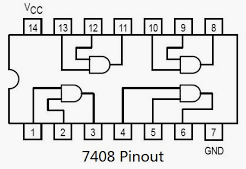
You will need to connect to a 7408 AND chip, using switch PB1 or PB2 as your clock. The 7408 chip is inserted BELOW the 7402 chip you wired in the previous exercise, and uses the following pin-out:
Verify the correct operation of the latch as follows:
Without pushing the clock button, set S=0 and R=0. Then flip through all four combinations of S and R. Why didn’t the outputs change?
Example answer: Without the clock on, the latch part just sees both inputs as 0s, since neither AND gate activates.
Set S=1 and R=0, then push and release the clock button. What is the value of Q? 0
1Now set S=0 and R=1, and push the clock button again. What is the value of Q? 0
1Did Q change when the button was pressed in, or when it was released (test again if you need to)? When it was pressed (rising edge).
When it was released (falling edge).Now set S=0 and R=0, and push the button. What is the value of Q? 0
1Without pressing the clock, flip S on and then off again. When it’s off, press the clock. Did Q’s value change? no
yesSet S=1 and R=1, and push and hold the button. Observe the value of Q while holding the button, and then release it. Explain why you cannot predict the value of Q after the button is released:
Example answer: This is the same situation as before, where with both NOR gates inactive due to active inputs from S and R, if you simultaneously turn those inputs off (such as by turning off the clock signal that’s connected to both), the system enters an unstable state. Whichever gate activates faster will stabilize it, but it’s not easy to predict which gate will win.