
🔬 Lab
CS 240 Lab 5
Processor Datapath
CS 240 Lab 5
In this lab, you will construct part of the hardware (called the datapath) for a simple computer. (referred to as the HW Arch). You have already studied some of the circuits that are major components in previous labs, including multiplexers, ALUs, registers, and register files.
To start with, use this simulator link to open the “CircuitVerse” simulator. It may take a while to load, with the progress bar getting stuck around halfway for a while. If this happens, open the dev tools and turn profiling on and off (ask for help if you’re not sure how to do that).
Next, download this circuit file and use the “Project -> Import File” option to load it into the simulator. We’ll use different sub-circuits in different parts of the lab.
Note: It’s important to select “Project -> Preview Circuit” for this lab when testing things because some outputs seem to randomly reset themselves otherwise.
Random-Access Memory
This exercise will show you how a RAM device is used to store and retrieve values from memory.
A RAM has different input/output capabilities compared to a register file: it has a single address input, a single data in input, and a single data out output, along with reset and write inputs.
A register file has three address inputs (read register 1, read register 2, and write register), while a RAM only has one. Which of the following is true as a consequence:
A RAM
can only write to the same address it’s reading from, while a register
file can read from one register while writing to
another.
A
register file can read from two different registers at once, while a RAM
can only read from a single memory cell.
A
register file can supply two different inputs to an ALU in a single
clock cycle, while a RAM cannot.
A
register file is much more expensive to manufacture per register, since
the addressing logic is more complex and each register needs two sets of
output wires.
Select the “RAM Test” tab of the HW ISA circuit, then select “Preview Circuit” from the “Project” menu.
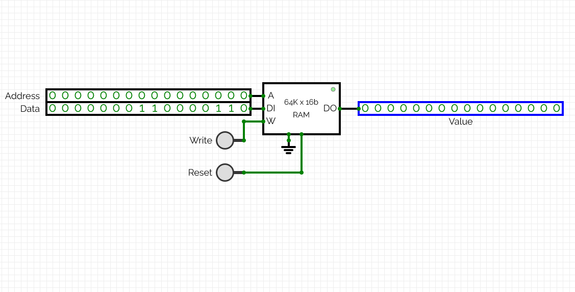
This circuit can be used to store data into a RAM at specific addresses, with the current value being overwritten by incoming data when the “Write” button is pressed.
Examine the circuit carefully to understand its operation: you write data values into a memory location specified by an address by using the inputs on the left to specify the data and address.
The hex displays show the values of the data input that you specify and the current data output of the RAM.
Exercise 1:
First, click on the RAM chip in the middle to
select it and then click on “Load Data” from the properties menu on the
right. Paste in the following values and hit “Ok”:
0x5002,0x5003,0x5003,0x0230. Then, toggle one of the
Address bits back and forth to get it to refresh.
To read from memory:
- Set the Address bits to the address you want by clicking to turn ones into zeroes or vice versa.
- View the value displayed in binary in the “Value” output on the right and in hexadecimal on the hex displays below that.
Read the data at addresses 0 through 3, and confirm it below (enter just the 4 hex digits you see, from top to bottom):
GCorrect answer:
Address 0000: Correct answer: 5002
Address 0001: Correct answer: 5003
Address 0002: Correct answer: 5003
Address 0003: Correct answer: 0230
Correct answer: See above
To write into the RAM, select the address you want to write to, set the data input to the desired new value for that address, and toggle the Write input on and then off again (by clicking the button).
Try writing the value 0x0123 into address 4 now.
Given that the RAM has 16 address inputs, how many storage slots does it have (i.e., how many distinct addresses are possible)?
Correct answer: 65536
Fetching Instructions
The “Arithmetic Cycle” circuit we saw in the pre-lab needs to be fed a series of instructions. A RAM could be used to store them. By feeding instructions one at a time into register file + ALU combo, we can run a program. This means we need to keep track of the current instruction, and have a mechanism for loading subsequent instructions one at a time.
The Program Counter or PC is used for this purpose: it’s a register that determines which instruction to read, and that increases its value every clock cycle.
The PC is connected to the address inputs of a RAM called “instruction memory,” so that the instruction stored at that address is output on the data output lines (and is then fed into the processor for execution).
The PC must be updated after an instruction is fetched, with the address of the next instruction stored in memory. Often, this will simply be PC + 2, since the default is that instructions execute in sequential order. An adder can accomplish this, as shown below:

Exercise 2:
Select the “PC Assembly” tab in CircuitVerse. Then select the RAM chip in the middle at the bottom, select “Load Data” from the “Properties” menu, and paste the following data:
0x5012,0xFFFF,0x5013,0xFFFF, 0x0040,0xFFFF,0x2232,0xFFFF, 0x2233,0xFFFF,0x3414,0xFFFF, 0x7401,0xFFFF,0x8003
Part of the circuit needs to add 2 to the current PC value, but the number ‘2’ doesn’t show up in the circuit diagram. Which part of the circuit represents the number 2 that we’ll use for adding to the current address each cycle, and how?
Hints:
- Remember that a diagonal wire attached to a group of numbered wires is a “breakout” which splits a bus (multiple wires bundled together) into smaller bundles (potentially just single wires).
- Also, a group of wires can represent a number if we have a pattern of low & high voltage (interpreted as binary ones and zeroes).
- The upward-pointing triangle symbol represents a connection to high-voltage, while the three lines below each other represent a connection to ground/low-voltage.
The breakout at the top of the circuit breaks a 16-wire bundle into
16 individual wires, of which we connect wire 1 (the 2’s place) to +5V
(1) and all the other wires to ground (0). This represents the binary
number 10 (with 14 leading zeroes) which is the decimal
number 2.
We can connect the bottom part of the diagonal wire attached to the breakout to wherever we need the number 2 as an input.
Hint: Recall that a row of wires with numbers on them represents breaking a multi-wire bus into smaller groups and/or single wires. Also, the upwards triangle in CircuitVerse represents +5V, i.e., logical 1, while the three bars represents ground which is logical 0.
This next step requires a bit more independent inference than usual. Ask the instructor for help if you’re not sure how to proceed.
Make the necessary connections to the circuit in CircuitVerse to implement instruction fetch according to the diagram above.
Remember that the purpose of this circuit is to set up an automatically incrementing “address” value and then feed that to a RAM chip so that instructions will be read out from the RAM one by one.
Once your circuit is hooked up, check if you get the right answers to the next two questions below, and check your results against the “Simple PC” tab if not.
- When the adder adds 2 to the PC register, it stores the result back
into that register. We’ve hooked up a 16-bit hex display on the left to
the “data in” input for the register, so you can see the value that will
be written to the register when the clock is toggled. When the
register’s output value is
0, what is the 4-digit hex value of this next-address-to-use bus? Correct answer: 0002 - If you click and release the “CLK” button, what new 4-digit hex value is shown in the top hex display on the right that shows the current value of the register? Correct answer: 0002? What value is now shown on the left waiting to be the next value for the register? Correct answer: 0004
Since the adder output is connected to the PC input, the PC output will update to match. Since the result of “PC + 2” is being stored back into the PC, we might worry that this will be an “infinite loop” in the circuit, immediately adding infinity to the PC since each result updates the value. Why doesn’t this happen?
Example answer: The PC register only updates itself at the instant when the clock signal falls from high to low. And during that update, the new stored value isn’t sent out of the output side until the input side is once again not accepting updates. So when the clock signal falls, we do a single “PC = PC + 2” operation, and then we wait until the clock signal falls again to do the next one. It is an infinite loop over time, but it’s controlled by the clock signal. This is possible because of the behavior of D flip-flops, which are used inside the PC register.
Assuming that the PC register uses falling-edge triggered D flip-flops to store data internally, when will the PC outputs change values?
Continuously
while the clock signal is on.
Continuously
while the clock signal is off.
Once per
cycle, at some point during the ON part of the clock
signal.
Once
per cycle, exactly on the falling edge of the clock
signal.
Once per
cycle, exactly on the rising edge of the clock
signal.
When the PC is updated to have the value 2, what will
the value of the adder output be? Correct
answer: 4
Explain what would happen during a single clock tick if the PC register used D latches (which update continuously during the clock ON pulse) instead of D flip-flops (which update once exactly on an edge of the clock signal) to store data?
Example answer: If the PC register used D latches, the input value would immediately determine the output value, which would then change the input to the adder, changing its outputs and feeding back into the PC inputs. This loop would keep adding 2 continuously during the ON tick of the clock, resulting in an undefined (and definitely incorrect) PC value. By using D flip-flops, we guarantee that the data is read in only at one instant (when the clock tick ends), and that the old address value is output during the entire clock ON cycle.
Exercise 3:
To fetch the instructions from memory:
Pulse the CLK and then Reset inputs (click the buttons and release them). Note that the PC value is now 0.
To go to the next address, you will pulse the CLK input (click and release).
Record the address and instruction below, and then repeatedly clock and record results for 8 instructions (do NOT reset between clocks; you just need to reset once).
| Address | Instruction |
|---|---|
| 0x00 | Correct answer: 5012 |
| 0x02 | Correct answer: 5013 |
| 0x04 | Correct answer: 0040 |
| 0x06 | Correct answer: 2232 |
| 0x08 | Correct answer: 2233 |
| 0x0A | Correct answer: 3414 |
| 0x0C | Correct answer: 7401 |
| 0x0E | Correct answer: 8003 |
Instruction Set Architecture
Before we add further components to our CPU, let’s take a look at how these instructions in the instruction memory are supposed to be interpreted. The HW ISA is a specification that determines what the HW Arch circuit is supposed to do.
Exercise 4:
For the first instruction we saw above, 0x5012, use the HW ISA Instructions table shown below to translate it into assembly syntax.
Note: The Opcode, Rs, Rt, and Rd values together are encoded in 16 bits (4 bits = 1 hex digit each). The opcode bits are the most significant bits, while the Rd bits are least significant.
| Assembly Syntax | Meaning (R = register file, M = data memory) |
Opcode | Rs | Rt | Rd |
|---|---|---|---|---|---|
| ADD Rs, Rt, Rd | R[d] ← R[s] + R[t] | 0010 | s | t | d |
| SUB Rs, Rt, Rd | R[d] ← R[s] - R[t] | 0011 | s | t | d |
| AND Rs, Rt, Rd | R[d] ← R[s] & R[t] | 0100 | s | t | d |
| OR Rs, Rt, Rd | R[d] ← R[s] | R[t] | 0101 | s | t | d |
| LW Rt, offset(Rs) | R[t] ← M[R[s] + offset] | 0000 | s | t | offset |
| SW Rt, offset(Rs) | M[R[s] + offset] ← R[t] | 0001 | s | t | offset |
| BEQ Rs, Rt, offset | If R[s] == R[t] then PC ← PC + 2 + offset * 2 |
0111 | s | t | offset |
| JMP offset | PC ← offset * 2 | 1000 | offset | ||
| HALT | Stops the program | 1111 | ignored | ||
Note: The JMP offset is unsigned. All other offsets are signed.
Keep the HW ISA Instructions slide open in another tab for reference throughout the lab.
The assembly syntax for 0x5012: Correct answer: OR R0, R1, R2
According to the HW ISA specification, which register should 0x5012 store its result in?
R0
R1
R2
R3
Which registers does 0x5012 read values from?
R0
R1
R2
R3
Explain what the result of executing 0x5012 should be, in terms of changes to the contents of the register file:
Example answer: The value of register R2 would be set to 1, since R0 always holds 0 and R1 always holds 1, so 0 | 1 is 1.
Click here to see each instruction from the provided RAM translated into HW ISA assembly, along with an explanation of what it does:
| Address | Instruction | HW ISA Assembly | What it does: |
|---|---|---|---|
| 0x00 | 5012 | OR R0, R1, R2 | set R2 to 1 |
| 0x02 | 5013 | OR R0, R1, R3 | set R3 to 1 |
| 0x04 | 0040 | LW R4 0(R0) | load memory at 0x0 into R4 |
| 0x06 | 2232 | ADD R2, R3, R2 | add R2 and R3, store into R2 |
| 0x08 | 2233 | ADD R2, R3, R3 | add R2 and R3, store into R3 |
| 0x0A | 3414 | SUB R4, R1, R4 | subtract 1 from R4 |
| 0x0C | 7401 | BEQ R4, R0, 1 | skip next instruction if R4 is 0 |
| 0x0E | 8003 | JMP 3 | jump to PC address 6 |
| 0x10 | 1022 | SW R2, 2(R0) | store R2 in M at address 2-3 |
| 0x12 | 1034 | SW R3, 4(R0) | store R3 in M at address 4-5 |
| 0x14 | F000 | HALT | stops the program |
Note that we did not ask you to inspect the last three instructions listed above.
Basically, this is how a program is executed:
Initially, the program instructions are loaded into the instruction memory.
Then, the instruction fetch mechanism you just saw loads one instruction at a time (one instruction per clock cycle).
The rest of the CPU executes that instruction during the clock cycle, updating the register file, data memory, and/or program counter as specified by the HW ISA.
The CPU circuit needs to be fast enough to deliver correct outputs by the end of the clock cycle, when these outputs will be internalized by the D flip-flops in each memory component and a new instruction from the instruction memory will be sent to the CPU.
Fill in the table for the following program to show your understanding of the HW instructions at the machine code level:
| Address | Instruction | Operation | Rs | Rt | Rd/offset | Purpose | Check |
|---|---|---|---|---|---|---|---|
| 0: | 5012 | OR | R0 | R1 | R2 | Set R2 to 1 | |
| GCorrect answer: 2: | 5013 | Correct answer: OR | Correct answer: R0 | Correct answer: R1 | Correct answer: R3 | Set R3 to 1 | Correct answer: See above |
| GCorrect answer: 4: | 2232 | Correct answer: ADD | Correct answer: R2 | Correct answer: R3 | Correct answer: R2 | Add R2 and R3, overwriting R2 | Correct answer: See above |
| GCorrect answer: 6: | 2233 | Correct answer: ADD | Correct answer: R2 | Correct answer: R3 | Correct answer: R3 | Add R2 and R3, overwriting R3 | Correct answer: See above |
| GCorrect answer: 8: | 8002 | Correct answer: JMP | Correct answer: 2 | Jump to PC 0x04 | Correct answer: See above | ||
Describe the result (specific values of modified registers, plus the current PC value) after 10 clock cycles have happened starting from PC = 0.
Example answer: 10 instructions will run all 5 of the listed instructions, plus after jumping up (which happens twice) instructions at addresses 4 and 6 will run twice more each. The final PC will be 8 (ready to do the jump again) and the values of R2 and R3 will be 13 and 21, respectively.
Does this program ever stop?
Yes
No
To connect this to a programming language we’re familiar with, click here to show an example of C code which might compile into these instructions:
void fibonacci() {
    int x = 1, y = 1;
    while (1) {
        x = x + y;
        y = x + y;
    }
}
Control Flow
High-level programming constructs like conditionals, loops, and functions all require the ability to specify which instruction to run next rather than always advancing to the next instruction in the list. This is called a jump.
The HW ISA specifies two kinds of jump instruction: BEQ and JMP. JMP just sets the program counter to a specific value (encoded in the last 12 bits of the instruction). However, BEQ implements a conditional jump: if the two registers specified for comparison hold the same value, it jumps relative to the normal next instruction by an amount specified in the last 4 bits, but if not, it continues to the next instruction in order as usual.
The diagram below shows the additional logic for producing a branch address for the BEQ instruction:

The offset for BEQ (which comes from the last 4 bits of the instruction) specifies the number of slots away from the next instruction in memory (PC + 2) to jump to. The additional adder calculates a branch address = PC + 2 + 2 * offset.
A 2x16 MUX then selects whether the next address going back to the PC is PC+2 or the branch address.
The selection line to the MUX is based on two control lines: the Branch bit, which is true when a BEQ instruction is being executed, and the Zero bit, which is true when the contents of Rs and Rt are equal.
The Zero bit comes from the ALU: when the result produced by the ALU is 0, the Zero bit is set to 1 (we saw that in the ALU lab).
So, on a BEQ instruction, the ALU performs Rs - Rt, which will set the Zero bit to 1 only when the contents of Rs is equal to the contents of Rt.
Exercise 5:
You’ll find an implementation of this logic in the “Program Counter” tab in CircuitVerse (it just has one “Branch” input instead of “Branch” and “Zero”). Use it to answer the following questions:
With Advance and Branch set to 0, set Reset to 1 and then back to 0. What is the address value? Correct answer: 0
Toggle the Advance input on and then off again 3 times. What is the address value now (in decimal)? Correct answer: 6
Set Offset to
1101(i.e., -3) and toggle Advance again. What is the address value in decimal? Correct answer: 8Why didn’t the offset value affect it? Example answer: Since Branch is still 0, the offset result is discarded at the right-hand multiplexer.
Now set Branch to 1 and toggle the Advance input one more time. What is the address value now? Correct answer: 4
Explain why an offset of -3 produces this result: Example answer: The BEQ logic takes the offset and multiplies it by 2 using a left-shift before applying it. So -3 becomes -6. It also applies the usual +2 update before applying the offset, so in total we have 8 + 2 - 6 = 4.
Basic Datapath
The following diagram describes the basic datapath for executing the arithmetic and logic instructions:
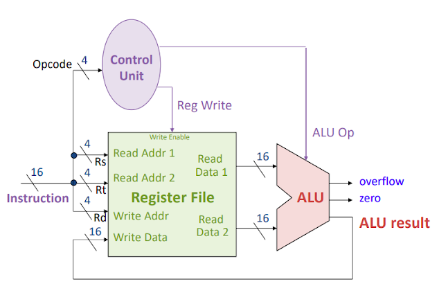
Exercise 6:
Select the “Datapath Assembly” tab in CircuitVerse.
Make the necessary connections to implement the diagram shown above. Don’t just make connections based on matching to the diagram, but also think about why each particular wire goes where it does (answer the questions below as you hook things up).
Where does each of the following signals go, and why?
Instruction bits 0-3: Register
File: Read 1
Register
File: Read 2
Register
File: Write Reg
Register
File: Write Data
Control Unit:
Opcode
ALU A
input
ALU B
input
Why? Example answer: These bits are the “Rd” or “destination register” part of the instruction, so they select which register to write to, and that’s what the “Write Reg” input to the register file does.
Instruction bits 4-7: Register
File: Read 1
Register
File: Read 2
Register
File: Write Reg
Register
File: Write Data
Control Unit:
Opcode
ALU A
input
ALU B
input
Why?
Example answer: These bits are the “Rt” part of the instruction, so they select one of the registers to read from. Using “Read 1” here would also work, at least for this part of the design.
Instruction bits 8-11: Register
File: Read 1
Register
File: Read 2
Register
File: Write Reg
Register
File: Write Data
Control Unit:
Opcode
ALU A
input
ALU B
input
Why?
Example answer: These bits are the “Rs” part of the instruction, so they select one of the registers to read from. Using “Read 2” here would also work, at least for this part of the design.
Instruction bits 12-15: Register
File: Read 1
Register
File: Read 2
Register
File: Write Reg
Register
File: Write Data
Control
Unit: Opcode
ALU A
input
ALU B
input
Why?
Example answer: These bits control which operation we perform. The control unit needs them to that it can control the other chips to perform that specific operation.
Register File: Data 1: Register
File: Read 1
Register
File: Read 2
Register
File: Write Reg
Register
File: Write Data
Control Unit:
Opcode
ALU A
input
ALU B
input
Why?
Example answer: These bits are read from a register (register number specified by the Read 1 input, which we hooked up to the Rs bits of the instruction) and need to get to the ALU so it can operate on them.
Register File: Data 2: Register
File: Read 1
Register
File: Read 2
Register
File: Write Reg
Register
File: Write Data
Control Unit:
Opcode
ALU A
input
ALU B
input
Why?
Example answer: These bits are read from a register (register number specified by the Read 2 input, which we hooked up to the Rt bits of the instruction) and need to get to the ALU so it can operate on them.
ALU: Result: Register
File: Read 1
Register
File: Read 2
Register
File: Write Reg
Register
File: Write Data
Control Unit:
Opcode
ALU A
input
ALU B
input
Why?
Example answer: The ALU result needs to be stored into the destination register so that we can access it in the future. The Write Reg input specifies which register to write to, and the ALU result gets sent to the Write Data input to specify what data to write.
Check your work against the “Datapath Assembled” tab in CircuitVerse.
The following table describes which ALU function will be produced by a given value of ALU Op:
| ALU Op | (decimal) | ALU function |
|---|---|---|
| 0000 | 0 | a AND b |
| 0001 | 1 | a OR b |
| 0010 | 2 | a + b (add) |
| 0110 | 6 | a - b |
BEQ is accomplished by subtraction (which sets the Zero bit).
BEQ and JMP do not change the value of a register.
The following table describes the ALU Op and Reg Write control lines for each type of instruction (note that in some cases different instructions use the same ALU operation):
| Instruction | Opcode | ALU Op | Reg Write |
|---|---|---|---|
| ADD | 0010 | 0010 | 1 |
| SUB | 0011 | 0110 | 1 |
| AND | 0100 | 0000 | 1 |
| OR | 0101 | 0001 | 1 |
| LW | 0000 | 0010 | 1 |
| SW | 0001 | 0010 | 0 |
| BEQ | 0111 | 0110 | 0 |
| JMP | 1000 | N/A | 0 |
| HALT | 1111 | N/A | N/A |
Simulate executing some instructions to verify that your circuit is correct:
- Pulse the “Reset” line (press and then release it) so that all registers are set to 0 (except R1 which always contains 1).
- Execute these tests in order without resetting in between.
- For each given test, set the specified values on the input devices and then pulse the CLK input (press and then release it) to execute the instruction.
- For each given instruction, record the values for each of the signals in the datapath, and note what registers are modified by the instruction.
- Then, to verify your result, set the inputs on the hex keyboards and switches in the circuit, and pulse the CLK to observe the output of the ALU.
Note: The ALU Op is not always the same as the opcode for an instruction- check the table directly above!
ADD R1,R1,R5
GCorrect answer:
Value Answer Opcode (in hex): Correct answer: 2 ALU Op (in hex): Correct answer: 2 s: Correct answer: 1 t: Correct answer: 1 d: Correct answer: 5 Reg Write: Correct answer: 1 ALU result (4 hex digits): Correct answer: 0002 Correct answer: See above
Which register is changed? Correct answer: R5
What value does that register have now (in decimal)? Correct answer: 2
ADD R5,R5,R2
GCorrect answer:
Value Answer Opcode (in hex): Correct answer: 2 ALU Op (in hex): Correct answer: 2 s: Correct answer: 5 t: Correct answer: 5 d: Correct answer: 2 Reg Write: Correct answer: 1 ALU result (4 hex digits): Correct answer: 0004 Correct answer: See above
Which register is changed? Correct answer: R2
What value does that register have now (in decimal)? Correct answer: 4
OR R2 R5 R6
GCorrect answer:
Value Answer Opcode (in hex): Correct answer: 5 ALU Op (in hex): Correct answer: 1 s: Correct answer: 2 t: Correct answer: 5 d: Correct answer: 6 Reg Write: Correct answer: 1 ALU result (4 hex digits): Correct answer: 0006 Correct answer: See above
Which register is changed? Correct answer: R6
What value does that register have now (in decimal)? Correct answer: 6
SUB R5,R6,R3
GCorrect answer:
Value Answer Opcode (in hex): Correct answer: 3 ALU Op (in hex): Correct answer: 6 s: Correct answer: 5 t: Correct answer: 6 d: Correct answer: 3 Reg Write: Correct answer: 1 ALU result (4 hex digits): Correct answer: FFFC Correct answer: See above
Which register is changed? Correct answer: R3
What value does that register have now (in decimal)? Correct answer: -4
AND R2,R5,R7
GCorrect answer:
Value Answer Opcode (in hex): Correct answer: 4 ALU Op (in hex): Correct answer: 0 s: Correct answer: 2 t: Correct answer: 5 d: Correct answer: 7 Reg Write: Correct answer: 1 ALU result (4 hex digits): Correct answer: 0000 Correct answer: See above
Which register is changed? Correct answer: R7
What value does that register have now (in decimal)? Correct answer: 0
Full Datapath with Memory Access Instructions
The following diagram adds the logic and the Data Memory device needed to implement the memory access instructions (LW and SW):
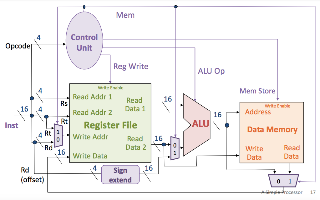
To distinguish between what is done in the dataptath for arithmetic/logic and control flow instructions (ADD, SUB, AND, OR, BEQ) versus what is done for memory access instructions (LW, SW), the following is necessary:
Use a 2x4 MUX at the input of the Register File to choose the source for the register to be written to (Rd gets written to for arithmetic/logic operations, Rt gets written to for LW).
Use a 2x16 MUX at the second input to the ALU. The MUX selects whether the ALU input comes from Rt or from the offset specified by the third operand of the instruction.
| Instruction | Datapath Action |
|---|---|
| ADD Rs Rt Rd | ALU performs Rs + Rt and stores result in Rd |
| SW Rs Rt offset | ALU performs Rs +
offset and sends result as Address to
Data Memory. Then value in Rt is stored to *Data Memory at specified address. |
| LW Rs Rt offset | ALU performs Rs +
offset and sends result as Address to
Data Memory. Then value at specified address in Data Memory is loaded to Rt. |
Exercise 7:
Below we have specified several operations by giving the relevant instruction values Rs, Rt, and Rd/offset as well as the Control Unit output values derived from the Opcode part of an instruction.
Refer to the table from the previous part about which ALU Op specifies which ALU function.
Before predicting the following operations, assume that all registers contain a value of 0 initially except R1 (which contains a 1). But assume that the registers are NOT reset between operations.
For each operation, first determine what HW ISA Opcode was used (enter these in decimal), and then predict the ALU result (in decimal) and explain which registers or memory locations would get a new value as a result of the operation.
Operation 1:
| ALU Op | s | t | d/offset | Reg Write | Mem | MemStore | Opcode (decimal) | ALU result |
|---|---|---|---|---|---|---|---|---|
| 2 | 1 | 1 | 6 | 1 | 0 | 0 | Correct answer: 2 | Correct answer: 2 |
Explain the operation and result, and what register is modified with what new value:
Example answer: Addition of R1 with itself. R1 + R1 = 1 + 1, stored in R6. R6 gets a 2.
Operation 2:
| ALU Op | s | t | d/offset | Reg Write | Mem | MemStore | Opcode (decimal) | ALU result |
|---|---|---|---|---|---|---|---|---|
| 2 | 6 | 6 | 3 | 1 | 0 | 0 | Correct answer: 2 | Correct answer: 4 |
Explain the operation and result:
Example answer: Addition of R6 with itself. R6 + R6 = 2 + 2, stored in R3. R3 gets a 4.
Operation 3:
| ALU Op | s | t | d/offset | Reg Write | Mem | MemStore | Opcode (decimal) | ALU result |
|---|---|---|---|---|---|---|---|---|
| 2 | 6 | 1 | 6 | 0 | 1 | 1 | Correct answer: 1 | Correct answer: 8 |
Explain how you figured out the opcode from the values of the control signals.
Example answer: Mem being 1 means it’s either LW or SW. MemStore being 1 means it’s SW.
What value would be stored to what address in Data Memory?
The value stored is from Rt, which is a 1, so the contents of register 1 are being copied into memory. That register always has the value 1.
The address to store to is given by the value of register Rs plus the offset specified where Rd would normally be given. So in this case, that’s Rs = R6, with value 2, plus offset = 6 gives us address 8.
Operation 4:
| ALU Op | s | t | d/offset | Reg Write | Mem | MemStore | Opcode (decimal) | ALU result |
|---|---|---|---|---|---|---|---|---|
| 2 | 3 | 6 | 4 | 1 | 1 | 0 | Correct answer: 0 | Correct answer: 8 |
Explain how you can figure out the opcode from the control signals:
Example answer: Mem being 1 means it’s either LW or SW. MemStore being 0 means it’s LW.
What address in Data Memory is being accessed?
Example answer: The address being accessed is address 8, the same one we just wrote to. But the way it’s computed is different. This time Rs = R3, and the offset is 4, so we compute 4 + 4 = 8.
What register will receive what new value from that address in Data Memory?
Example answer: R6 gets the value 1, which was previously stored in address 8.
Stretch Exercises: Control Unit
You have seen that the ALU Op bits (which control the operation of the ALU) are not the same as the instruction opcode (which specifies which instruction is being executed).
It is necessary to translate the instruction opcode to the proper ALU operation (which specifies ainv bneg op1 op0 into the ALU) for each instruction, as shown below:
| Instruction | opcode | ALU operation | ALU operation encoding | ||||||
| O3 | O2 | O1 | O0 | ainv | bneg | op1 | op0 | ||
| LW | 0 | 0 | 0 | 0 | ADD | 0 | 0 | 1 | 0 |
| SW | 0 | 0 | 0 | 1 | ADD | 0 | 0 | 1 | 0 |
| ADD | 0 | 0 | 1 | 0 | ADD | 0 | 0 | 1 | 0 |
| SUB | 0 | 0 | 1 | 1 | SUB | 0 | 1 | 1 | 0 |
| AND | 0 | 1 | 0 | 0 | AND | 0 | 0 | 0 | 0 |
| OR | 0 | 1 | 0 | 1 | OR | 0 | 0 | 0 | 1 |
| BEQ | 0 | 1 | 1 | 1 | SUB | 0 | 1 | 1 | 0 |
Note: The JMP instruction is not shown in this table because it does not use the ALU.
Exercise 8:
Explain why LW and SW have the same ALU operation as ADD:
Example answer: Because they need to add the address register to the offset that comes as part of the opcode to get the actual address to read from or write to.
Write a Boolean function for each ALU operation bit in terms of the opcode “O0-O3” inputs.
ainv = 0 (always off in these examples)
bneg = Example answer: O1O0
op1 = Example answer: O2’ + O2O1O0 (could be simplified to O2’ + O1)
op0 = Example answer: O2O1’O0
The logic to produce the ALU Op bits (which you just designed) is part of the Control Unit.
The Control Unit also produces the other data path control signals for each instruction, as shown below:
| Instruction | opcode | Reg Write | Mem | Mem Store | Branch | Jump | |||
| O3 | O2 | O1 | O0 | ||||||
| LW | 0 | 0 | 0 | 0 | 1 | 1 | 0 | 0 | 0 |
| SW | 0 | 0 | 0 | 1 | 0 | 1 | 1 | 0 | 0 |
| ADD | 0 | 0 | 1 | 0 | 1 | 0 | 0 | 0 | 0 |
| SUB | 0 | 0 | 1 | 1 | 1 | 0 | 0 | 0 | 0 |
| AND | 0 | 1 | 0 | 0 | 1 | 0 | 0 | 0 | 0 |
| OR | 0 | 1 | 0 | 1 | 1 | 0 | 0 | 0 | 0 |
| BEQ | 0 | 1 | 1 | 1 | 0 | 0 | 0 | 1 | 0 |
| JMP | 1 | 0 | 0 | 0 | 0 | 0 | 0 | 0 | 1 |
Explain why the Reg Write bit is set for LW, ADD, SUB, AND, OR, but not for SW, BEQ, or JMP:
Example answer: The operations where RegWrite is set are operations where a result is written to a register. SW, BEQ, and JMP don’t write to a register: SW writes to memory instead, and BEQ and JMP change the PC.
Write a boolean function for each control line as a function of the opcode bits O0-O3:
RegWrite = Example answer: (O3’O2’O1’O0 + O2O1O0 + O3)’
Mem = Example answer: O3’O2’O1’
Mem Store = Example answer: O3’O2’O1’O0
Branch = Example answer: O2O1O0
Jump = Example answer: O3
Although we will not do so in lab today, you can see that it is easy to implement the Control Unit with basic logic gates. The “Control Unit” tab in CircuitVerse has an example that uses multiplexers hooked up to constant inputs to specify which values each output should have for each possible instruction.
Extra Exercises: Full Implementation
Select the “Full CPU” tab in CircuitVerse.
Minimize the “Circuit Elements” and/or “Properties” windows in CircuitVerse to view the full circuit.
Click here for a description of the “Full CPU” circuit.
The Program Counter and Instruction Memory are on the left, with hex displays for the program counter on that circuit and the current instruction as well.
The instruction gets split into 4 groups of 4 bytes each, and we send one to the Control Unit while using the other three to set the read & write addresses of the Register File (with a multiplexer determining whether group 2 or group 3 sets the write address of the register file).
The outputs of the Register File go into the A and B inputs of the ALU, with another multiplexer that can swap the B input to get its value from bits 0-3 of the instruction (sign extended to 16 bits) instead of the second register value from the ALU.
The result of the ALU becomes the address for the Data Memory, as well as cycling back around to the “Write Data” input to the register file, although a multiplexer there can cause the data read from the data memory to be fed back into the register file instead.
The second register value also gets set to the “Data In” (DI) input of the data memory.
Hex displays show the two values read from registers, as well as the ALU result (or the value read from data memory if that’s being used instead of the ALU result).
The control unit has 7 outputs, which are:
- The “ALU Op” output is connected to the ALU, along with the “Invert A” and “Invert B & Carry” outputs (the last of which sets both the “Invert B” and “Carry In” inputs of the ALU).
- The “Mem” output controls the three multiplexers mentioned above, so
when active it causes:
- Bits 8-11 of the instruction are used for the write register of the register file instead of bits 0-3.
- Bits 0-3 are sign extended and used as the B input of the ALU instead of the data from the second register result of the register file.
- The RAM result is fed back into the write data of the register file instead of the ALU result.
- The “Mem Store” output controls whether the “write” input of the data memory is on or off.
- The “Reg Write” output controls the “Write Enable” input of the register file.
- The “Branch” output goes into an AND gate along with the “Zero” output of the ALU. That result is connected to the “Branch” input on the Program Counter.
- The “Jump” output of the control unit is not connected anywhere (this version of the CPU does not implement the JUMP instruction).
The Reset, CLK, and PC reset buttons on the left are used to control execution of a program in the CPU. The following program will perform a loop (the first three instructions initialize registers to values to be used in the calculation).
Exercise 9:
Fill in the hexadecimal value for each encoded instruction in the table below, including necessary values to make the BEQ instructions reach the intended lines:
| Address | Instruction | op | Rs, Rt, Rd/offset | Purpose |
|---|---|---|---|---|
| 0: | 2112 | ADD | R1, R1, R2 | ; R2 = 2 |
| 2: | Correct answer: 2223 | ADD | R2, R2, R3 | ; R3 = 4 |
| 4: | Correct answer: 2334 | ADD | R3, R3, R4 | ; R4 = 8 |
| 6: (LOOP) | Correct answer: 3424 | SUB | R4, R2, R4 | ; R4 <- R4 - R2 |
| 8: | Correct answer: 4444 | AND | R4, R4, R4 | ; display the result of the subtraction |
| A: | Correct answer: 7422 | BEQ | R4, R2, NEXT | ; escape the loop when R4 = 2 |
| C: | Correct answer: 700C | BEQ | R0, R0, LOOP | ; repeat the loop |
| … | ||||
| 10: (NEXT) | Correct answer: 1032 | SW | R0, R3, 2 | ; store 4 at address 2 in data memory |
| 12: | Correct answer: 1244 | SW | R2, R4, 4 | ; store 2 at address 6 in data memory |
| 14: | Correct answer: 0052 | LW | R0, R5, 2 | ; load 4 from address 2 in memory into R5 |
| 16: | Correct answer: 4555 | AND | R5, R5, R5 | ; display the contents of R5 = 4 |
| 18: | Correct answer: 5555 | OR | R5, R5, R5 | ; will also display 4 |
| 1A: | Correct answer: FFFF | HALT | don’t matter | ; halt execution |
Note that we could have used JUMP for the second BEQ, but the CircuitVerse implementation does not implement the JUMP instruction.
To load the Instruction Memory with this program, select the Instruction Memory RAM, hit “Load Data” (in the “Properties” menu on the right) and paste in the following:
0x2112,0xFFFF,0x2223,0xFFFF,0x2334,0xFFFF,
0x3424,0xFFFF,0x4444,0xFFFF,0x7422,0xFFFF,
0x700C,0xEEEE,0xEEEE,0xFFFF,0x1032,0xFFFF,
0x1244,0xFFFF,0x0052,0xFFFF,0x4555,0xFFFF,
0x5555
To execute the program:
- Press & release the Reset button.
- Press & release the Reset PC to 0 button.
- Press & release the CLK button to execute one instruction.
Stop the first time PC = 8, and examine the output of the ALU. The first time, you should see the value of 6 displayed at the ALU output.
Keep executing the program, examining the result each time PC = 8.
The program is finished when PC = 0x1A. How many times was the loop repeated? Correct answer: 3
Writing Programs
Exercise 10:
Write a program that does NOT use JUMP which sets the ALU result to a value of 0x1000 or higher.
There are many possible solutions, but it’s tricky because you only
start with the number 1 and there is no multiply operation. However, you
can do 0x2112 to compute 1 + 1 and store 2 into register 2.
Then you can do 0x2222 repeatedly to double that value by
adding it to itself. You could use a loop with BEQ to repeat that
step.
If you consider the ALU result to be unsigned, you can also just do
0x3012 to get 0xFFFF as the result.
Load your program into the CPU and test to make sure it works.
Exercise 11:
Note: in CircuitVerse, the JUMP instruction is not implemented, so while you can write these programs, you cannot execute them on the CPU.
Assume that after the previous exercise, you have a value of 4 stored in address 2 and a value of 2 stored in address 6 in Data Memory.
Write a program which will add those two values together, and store the result in address 0 in Data Memory. Write your program as a series of hexadecimal instructions in the table below, using registers 5 and 6 to store the data after loading it from memory, and register 7 to hold the addition result before loading it back into memory:
| Address | Instruction (hexadecimal) | Explanation |
|---|---|---|
| 0 | 0052 | Example answer: Load from address 2 into R5 |
| 2 | Correct answer: 0066 | Example answer: Load from address 6 into R6 |
| 4 | Correct answer: 2567 | Example answer: Add R5 + R6 and store in R7 |
| 6 | Correct answer: 1070 | Example answer: Store R7 in memory address 0 |
Load your program into the Instruction Memory and verify that it works correctly.
Now, write a program which will load from memory addresses 2 and 6 and multiply those two values using a loop with successive addition (use the R2 and R3 registers to hold the loaded values, and R4 for the result. Record your program below:
| Address | Instruction (hexadecimal) | Explanation |
|---|---|---|
| 0 | 0022 | Example answer: Load from address 2 into R2 |
| 2 | Correct answer: 0036 | Example answer: Load from address 6 into R3 |
| 4 | Correct answer: 5004 | Example answer: Zero out R4 |
| 6 | Correct answer: 2244 | Example answer: Add R2 and R4, overwriting R4 |
| 8 | Correct answer: 3313 | Example answer: Subtract 1 from R3, updating it |
| A | Correct answer: 7301 | Example answer: Skip the following JMP if R3 is 0 |
| C | Correct answer: 8003 | Example answer: Jump back to address 6, to add again |
| E | Correct answer: FFFF | Example answer: Halt |
Note that at the end, you can use instruction 4444 to show register 4 which should hold the result.
Load your program into the Instruction Memory and verify that it works correctly.