
🔬 Lab
CS 240 Lab 5
Processor Datapath
CS 240 Lab 5
In this lab, you will construct part of the hardware (called the datapath) for a simple computer. (referred to as the HW Arch). You have already studied some of the circuits that are major components in previous labs, including multiplexers, ALUs, registers, and register files.
Random-Access Memory
If you already did this part but your partner hasn’t, walk through it again together. If both of you have already done it, you should skip it.
This exercise will show you how a RAM device is used to store and retrieve values from memory.
Download this instructionMemory.cct circuit and then open it in LogicWorks:
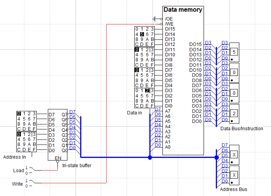
This circuit can be used to store data into addresses of a RAM memory, which is necessary for loading a program into the instruction memory.
Examine the circuit carefully to understand its operation: you write data values into a memory location specified by an address by using the hex keyboards on the left to specify the data and address.
The currently selected address and the value stored at that address are displayed on the hex displays on the right.
Exercise 1:
To read from memory: 1. Set Load to 0 (the Load line connects the address switches to the memory chip through the tri-state buffers, which let a signal through only when Load is set to 0. When inactive, the tri-state buffers have neither high nor low output, which LogicWorks shows as an ‘X’). 2. Select the address you want to read from on the Address in keyboards. 3. The data at that address will appear on the Data bus at the right.
Read the data at addresses 0 through 3, and confirm it below (enter just the 4 hex digits you see, from top to bottom):
GCorrect answer:
Address 00: Correct answer: 5002
Address 01: Correct answer: 5003
Address 02: Correct answer: 5003
Address 03: Correct answer: 0230
Check AnswersCorrect answer: See above
Exercise 2:
To write to memory (load a program): 1. Set Load to 0. 2. Set the Address switches to the location in memory at which you wish to write a data value. 3. Set the Data switches to the value you wish to write to that location. 4. Set Write to 0, then back to 1 (writes the data input into the specified address in memory). 5. Repeat steps 2 - 4 for each address and its data value.
Using the write procedure, load the following data values to the specified addresses:
| Addr | Data |
|---|---|
| 00 | 5002 |
| 02 | 5003 |
| 04 | 1220 |
| 06 | 0230 |
| 08 | 2122 |
| 0A | 8001 |
As you write the values, you will observe the address and data values on the data and address bus displays. At any time, you can observe the contents of an address by setting the address switches to the desired location (without toggling the Write switch).
When you are finished, set Load = 1 to disable the address inputs.
This will always be required when the user is finished loading the program into memory, and wishes to run the program. When RAM is used as part of a full computer, the address is supplied by the CPU during execution of the program, so the switches are not needed at that point (and would interfere with the CPU operation if still connected).
Given that the RAM has 8 address inputs, how many values can it store? Correct answer: 256
Which part(s) of this RAM would it make sense to hook up to which part(s) of an ALU in a design for a full computer (there are several good answers here)?
Example answer: The “Data in” could be hooked up to an ALU’s result to store that result in memory. Similarly, the “Data bus” outputs could be hooked up to one of the inputs of an ALU in order to use data from memory as part of an operation. Although less obvious, the address bus could serve as input and/or output as well, if we need to compute the address of some data using a formula. For example, using the address as one input and the number 1 as another input and setting the ALU to do addition, we could compute the next higher address as part of a solution for writing multiple values into sequential addresses. Finally, one could hook part of the data bus outputs into the Operation bits of the ALU, to let the data determine what operation the ALU will perform!
Fetching Instructions
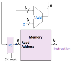
The RAM we just saw can be used to store a program, if each word stored corresponds to an HW ISA instruction. By feeding these instructions one at a time into a CPU, we can run that program. This means we need to keep track of the current instruction, and have a mechanism for loading subsequent instructions one at a time. The Program Counter or PC is used for this purpose: it’s a register that determines which instruction to read, and that increases its value every clock cycle.
The PC is connected to the address inputs of the memory device, and the instruction stored at that address is output on the data output lines of the memory device (and is then fed into the processor for execution).
The PC must be updated after an instruction is fetched, with the address of the next instruction stored in memory. Often, this will simply be PC + 2, since the default is that instructions execute in sequential order. An adder can accomplish this, as shown below:
Exercise 3:
Download the FetchInstruction.cct circuit and then open it in LogicWorks.
The memory has been loaded with a program previously, by writing data representing instructions to sequential addresses in memory, starting at address 0 (as you did in the previous exercise).
Make the necessary connections to the circuit shown below to implement instruction fetch (look at the previous diagram to understand where to make the connections in the circuit).
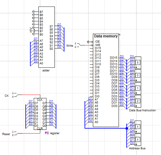
When you’ve made the connections, check them against this image (there are three connections to make).
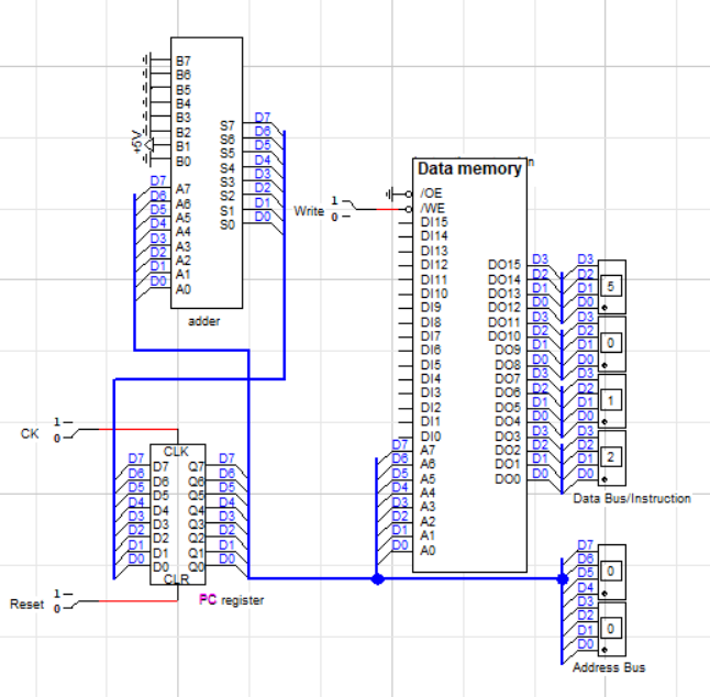
Describe how the value of “2” is achieved as an input to the adder in the circuit:
Example answer: The B1 line is set to +5V while the rest of the B lines are set to ground, meaning that the inputs B0 through B7 are permanently set to 0000 0010, which represents the number 2.
When the adder adds 2 to the PC, it stores the result back into the
PC. Turn on “Simulation -> Show Values” in LogicWorks and you’ll be
able to see the data values each bus is carrying as hex digits. When the
PC output value is 00, what is the value of the output from
the adder? Correct
answer: 02
Since the adder output is connected to the PC input, the PC output will update to match. Given that the PC register uses D flip-flops to store data internally, when will this happen?
Continuously
while the clock signal is on.
Continuously
while the clock signal is off.
Once per
cycle, at some point during the ON part of the clock
signal.
Once
per cycle, exactly on an edge of the clock
signal.
When the PC is updated to have the value 02, what will
be the value of the adder ouptut? Correct
answer: 04
Explain what would happen during a single clock tick if the PC register used D latches (which update continuously during the clock ON pulse) instead of D flip-flops (which update once exactly on the falling edge of the clock) to store data?
Example answer: If the PC register used D latches, the inputs D0-D7 would immediately determine the outputs Q0-Q7, which would then change the input to the adder, changing its outputs and feeding back into the D0-D7 inputs. This loop would keep adding 2 continuously during the ON tick of the clock, resulting in an undefined (and definitely incorrect) PC value. By using D flip-flops, we guarantee that the data is read in only at one instant (when the clock tick ends), and that the old address values are output during the entire clock ON cycle.
Exercise 4:
To fetch the instructions from memory:
Pulse the Reset input (1 then back to 0). Note that PC = 0 (same as the address).
Activate the CK (set to 1 and back to 0) to go to the next address.
Record the address and instruction below, and then repeatedly clock and record results for 8 instructions (do NOT reset between clocks; you just need to reset once).
| Address | Instruction |
|---|---|
| 0x00 | Correct answer: 5012 |
| 0x02 | Correct answer: 5013 |
| 0x04 | Correct answer: 0040 |
| 0x06 | Correct answer: 2232 |
| 0x08 | Correct answer: 2233 |
| 0x0A | Correct answer: 3414 |
| 0x0C | Correct answer: 7401 |
| 0x0E | Correct answer: 8003 |
Instruction Set Architecture
Before we add further components to our CPU, let’s take a look at how these instructions in the instruction memory are supposed to be interpreted. The HW ISA is a specification that determines what the HW Arch circuit is supposed to do.
Exercise 5:
For the first instruction we saw above, 0x5012, use the HW ISA Instructions table shown below to translate it into assembly syntax.
Note: The Opcode, Rs, Rt, and Rd values together are encoded in 16 bits (4 bits = 1 hex digit each). The opcode bits are the most significant bits, while the Rd bits are least significant.
| Assembly Syntax | Meaning (R = register file, M = data memory) |
Opcode | Rs | Rt | Rd |
|---|---|---|---|---|---|
| ADD Rs, Rt, Rd | R[d] ← R[s] + R[t] | 0010 | s | t | d |
| SUB Rs, Rt, Rd | R[d] ← R[s] - R[t] | 0011 | s | t | d |
| AND Rs, Rt, Rd | R[d] ← R[s] & R[t] | 0100 | s | t | d |
| OR Rs, Rt, Rd | R[d] ← R[s] | R[t] | 0101 | s | t | d |
| LW Rt, offset(Rs) | R[t] ← M[R[s] + offset] | 0000 | s | t | offset |
| SW Rt, offset(Rs) | M[R[s] + offset] ← R[t] | 0001 | s | t | offset |
| BEQ Rs, Rt, offset | If R[s] == R[t] then PC ← PC + 2 + offset * 2 |
0111 | s | t | offset |
| JMP offset | PC ← offset * 2 | 1000 | offset | ||
| HALT | Stops the program | 1111 | ignored | ||
Note: The JMP offset is unsigned. All other offsets are signed.
Keep the HW ISA Instructions slide open in another tab for reference throughout the lab.
The assembly syntax for 0x5012: Correct answer: OR R0, R1, R2
We haven’t shown you the register file yet, but you’ve seen the HW ISA, which is a specification for what the HW Arch circuit must do. According to the specification, which register should 0x5012 store its result in?
R0
R1
R2
R3
Which registers does 0x5012 read values from?
R0
R1
R2
R3
Explain what the result of executing 0x5012 should be, in terms of changes to the contents of the register file:
Example answer: The value of register R2 would be set to 1, since R0 always holds 0 and R1 always holds 1, so 0 | 1 is 1.
After working through the exercises above, click here to see each instruction from the provided RAM translated into HW ISA assembly, along with an explanation of what it does:
| Address | Instruction | HW ISA Assembly | What it does: |
|---|---|---|---|
| 0x00 | 5012 | OR R0, R1, R2 | set R2 to 1 |
| 0x02 | 5013 | OR R0, R1, R3 | set R3 to 1 |
| 0x04 | 0040 | LW R4 0(R0) | load memory at 0x0 into R4 |
| 0x06 | 2232 | ADD R2, R3, R2 | add R2 and R3, store into R2 |
| 0x08 | 2233 | ADD R2, R3, R3 | add R2 and R3, store into R3 |
| 0x0A | 3414 | SUB R4, R1, R4 | subtract 1 from R4 |
| 0x0C | 7401 | BEQ R4, R0, 1 | skip next instruction if R4 is 0 |
| 0x0E | 8003 | JMP 3 | jump to PC address 6 |
| 0x10 | 1022 | SW R2, 2(R0) | store R2 in M at address 2-3 |
| 0x12 | 1034 | SW R3, 4(R0) | store R3 in M at address 4-5 |
| 0x14 | F000 | HALT | stops the program |
Note that we did not ask you to inspect the last three instructions listed above.
Basically, this is how a program is executed:
Initially, the program instructions are loaded into the instruction memory.
Then, the instruction fetch mechanism you just saw loads one instruction at a time (one instruction per clock cycle).
The rest of the CPU executes that instruction during the clock cycle, updating the register file, data memory, and/or program counter as specified by the HW ISA.
The CPU circuit needs to be fast enough to deliver correct outputs by the end of the clock cycle, when these outputs will be internalized by the D flip-flops in each memory component and a new instruction from the instruction memory will be sent to the CPU.
Fill in the table for the following program to show your understanding of the HW instructions at the machine code level:
| Address | Instruction | Operation | Rs | Rt | Rd/offset | Purpose | Check |
|---|---|---|---|---|---|---|---|
| 0: | 5012 | OR | R0 | R1 | R2 | Set R2 to 1 | |
| GCorrect answer: 2: | 5013 | Correct answer: OR | Correct answer: R0 | Correct answer: R1 | Correct answer: R3 | Set R3 to 1 | Check AnswersCorrect answer: See above |
| GCorrect answer: 4: | 2232 | Correct answer: ADD | Correct answer: R2 | Correct answer: R3 | Correct answer: R2 | Add R2 and R3, overwriting R2 | Check AnswersCorrect answer: See above |
| GCorrect answer: 6: | 2233 | Correct answer: ADD | Correct answer: R2 | Correct answer: R3 | Correct answer: R3 | Add R2 and R3, overwriting R3 | Check AnswersCorrect answer: See above |
| GCorrect answer: 8: | 8002 | Correct answer: JMP | Correct answer: 2 | Jump to PC 0x04 | Check AnswersCorrect answer: See above | ||
Describe the result (specific values of modified registers, plus the current PC value) after allowing 10 total instructions to execute:
Example answer: 10 instructions will run all 5 of the listed instructions, plus after jumping up (which happens twice) instructions at addresses 4 and 6 will run twice more each. The final PC will be 8 (ready to do the jump again) and the values of R2 and R3 will be 13 and 21, respectively.
Does this program ever stop?
Yes
No
To connect this to a programming language we’re familiar with, click here to show an example of C code which might compile into these instructions:
void fibonacci() {
    int x = 1, y = 1;
    while (1) {
        x = x + y;
        y = x + y;
    }
}
Control Flow
As you learned about in lecture and the pre-lab assignment for today, the logic of conditional execution in the HW computer is implemented by BEQ and JMP instructions.
The diagram below shows the additional logic for producing a branch address for the BEQ instruction:
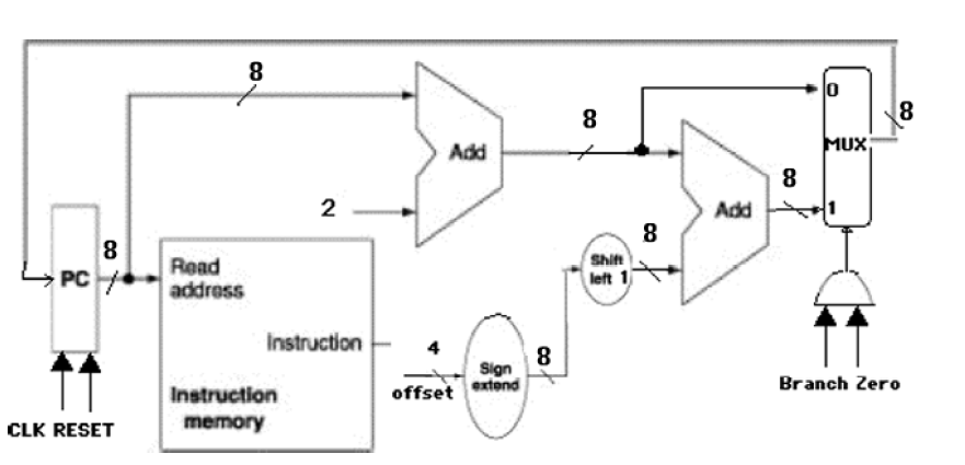
The offset for BEQ (which comes from the last 4 bits of the instruction) specifies the number of words away from the next instruction in memory (PC + 2) to jump to. The additional adder calculates a branch address = PC + 2 + 2 * offset.
A 2x8 MUX then selects whether the next address going back to the PC is PC+2 or the branch address.
The selection line to the MUX is based on two control lines: the Branch bit, which is true when a BEQ instruction is being executed, and the Zero bit, which is true when the contents of Rs and Rt are equal.
The Zero bit comes from the ALU: when the result produced by the ALU is 0, the Zero bit is set to 1 (we saw that in the ALU lab).
So, on a BEQ instruction, the ALU performs Rs - Rt, which will set the Zero bit to 1 only when the contents of Rs is equal to the contents of Rt.
Exercise 6:
Download the ControlFlow.cct circuit and then open it in LogicWorks.
Connect together the components in the circuit to implement the branch address logic as shown in the diagram above.
You will use the switches and hex keyboard you are given in the circuit to simulate Branch, Zero and the 4-bit BEQ offset (the real signals are produced in parts of the CPU we haven’t added yet).
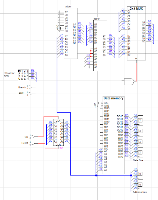
When the circuit is complete, pulse the Reset line (set to 1 and back to 0) to initialize the PC to address 0. (Do NOT reset for each of the following exercises, instead just do this one to set things up).
Set the offset = 3, Branch = 1, and Zero = 1 and pulse the CK (set to 1 and back to 0):
What is the value of the PC (two hex digits)? Correct answer: 08
Click here to see what the circuit should look like when it’s connected:
Now set Zero = 0 for the next instruction (without resetting the PC, which should match the answer above). Activate the CK.
What is the value of the PC? Correct answer: 0A Why? Example answer: If the Zero bit is not set, that implies the two values were not equal, so the branch shouldn’t happen. Instead, the normal PC = PC + 2 formula kicks in.
Set Branch = 0 and Zero = 1 for the next instruction. Activate the CK.
What is the value of the PC? Correct answer: 0C Why? Example answer: The Branch but must be set in addition to the Zero bit for a jump to happen.
Set Branch = 1 and Zero = 1, and set offset to each of the following values for the next set of instructions (you should see that PC = 0C to begin):
Note: Offset is a 4-bit two’s complement values (so can be negative!), and both offset and PC are displayed in hexadecimal notation.
Record the PC for each offset after activation of the CK. Write the formula you used to calculate your result in the right column.
| offset | PC (in hex with ‘0x’) | Formula used |
|---|---|---|
| 0xC | Correct answer: 0x06 | Example answer: C + 2 + 2*(-4) = E - 8 = 6 |
| 0x5 | Correct answer: 0x12 | Example answer: 6 + 2 + 2*5 = 8 + 10 = 18 = 0x12 |
| 0x2 | Correct answer: 0x18 | Example answer: 0x12 + 2 + 2*2 = 0x14 + 4 = 0x18 |
Basic Datapath
The following diagram describes the basic datapath for executing the arithmetic and logic instructions:
Exercise 7:
Download the datapath.cct circuit and then open it in LogicWorks.
Make the necessary connections to implement the diagram shown above. Make sure to turn on “Simulation -> Show Values.”
Note that we do not have a control unit, and instead control the ALU Op and RegWrite values directly
Click here to check your work:
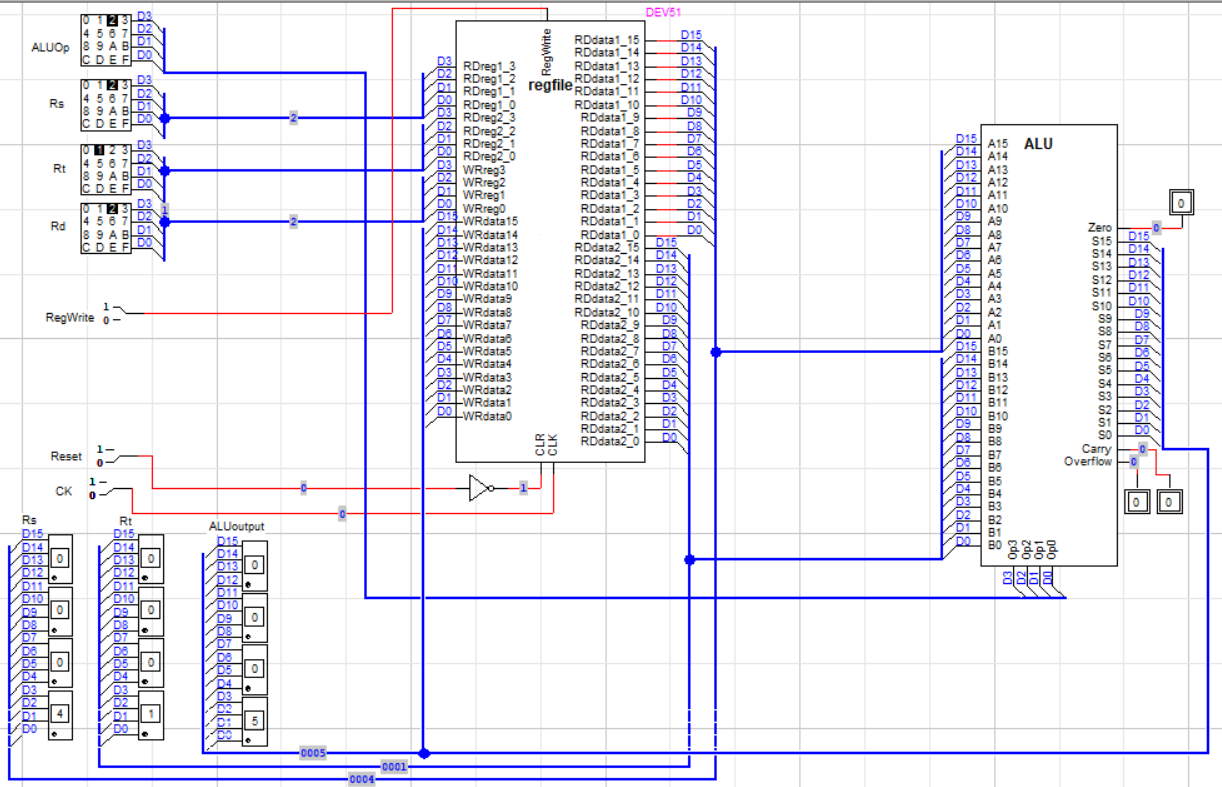
The following table describes which ALU function will be produced by a given value of ALUOp:
| ALU Op | (decimal) | ALU function |
|---|---|---|
| 0000 | 0 | a AND b |
| 0001 | 1 | a OR b |
| 0010 | 2 | a + b (add) |
| 0110 | 6 | a - b |
BEQ is accomplished by subtraction (which sets the Zero bit).
BEQ and JMP do not change the value of a register.
The following table describes the ALU Op and Reg Write control lines for the arithmetic/logic and control flow instructions:
| Instruction | Opcode | ALU Op | Reg Write |
|---|---|---|---|
| ADD | 0010 | 0010 | 1 |
| SUB | 0011 | 0110 | 1 |
| AND | 0100 | 0000 | 1 |
| OR | 0101 | 0001 | 1 |
| BEQ | 0111 | 0110 | 0 |
| JMP | 1000 | N/A | 0 |
Simulate executing some instructions to verify that your circuit is correct:
- Pulse the “Reset” line (set it to 1 and then back to 0) so that all registers are set to 0 (except R1 which always contains 1).
- Execute these tests in order without resetting in between.
- For each given test, set the specified values on the input devices and then pulse the CLK input (set to 1 and back to 0) to execute the instruction.
- For each given instruction, record the values for each of the signals in the datapath, and note what registers are modified by the instruction.
- Then, to verify your result, set the inputs on the hex keyboards and switches in the circuit, and pulse the CLK to observe the output of the ALU.
Note: The ALUop is not always the same as the opcode for an instruction- check the table directly above!
ADD R1,R1,R5
ALUop (in hex): Rs: Rt: Rd: RegWrite: ALU result (4 hex digits): GCorrect answer: Correct answer: 2 Correct answer: 1 Correct answer: 1 Correct answer: 5 Correct answer: 1 Correct answer: 0002 Check AnswersCorrect answer: See above
Which register is changed? Correct answer: R5
What value does that register have now (in decimal)? Correct answer: 2
ADD R5,R5,R2
ALUop (in hex): Rs: Rt: Rd: RegWrite: ALU result (4 hex digits): GCorrect answer: Correct answer: 2 Correct answer: 5 Correct answer: 5 Correct answer: 2 Correct answer: 1 Correct answer: 0004 Check AnswersCorrect answer: See above
Which register is changed? Correct answer: R2
What value does that register have now (in decimal)? Correct answer: 4
OR R2 R5 R6
ALUop (in hex): Rs: Rt: Rd: RegWrite: ALU result (4 hex digits): GCorrect answer: Correct answer: 1 Correct answer: 2 Correct answer: 5 Correct answer: 6 Correct answer: 1 Correct answer: 0006 Check AnswersCorrect answer: See above
Which register is changed? Correct answer: R6
What value does that register have now (in decimal)? Correct answer: 6
SUB R5,R6,R3
ALUop (in hex): Rs: Rt: Rd: RegWrite: ALU result (4 hex digits): GCorrect answer: Correct answer: 6 Correct answer: 5 Correct answer: 6 Correct answer: 3 Correct answer: 1 Correct answer: FFFC Check AnswersCorrect answer: See above
Which register is changed? Correct answer: R3
What value does that register have now (in decimal)? Correct answer: -4
AND R2,R5,R7
ALUop (in hex): Rs: Rt: Rd: RegWrite: ALU result (4 hex digits): GCorrect answer: Correct answer: 0 Correct answer: 2 Correct answer: 5 Correct answer: 7 Correct answer: 1 Correct answer: 0000 Check AnswersCorrect answer: See above
Which register is changed? Correct answer: R7
What value does that register have now (in decimal)? Correct answer: 0
Full Datapath with Memory Access Instructions
The following diagram adds the logic and the Data Memory device needed to implement the memory access instructions (LW and SW):
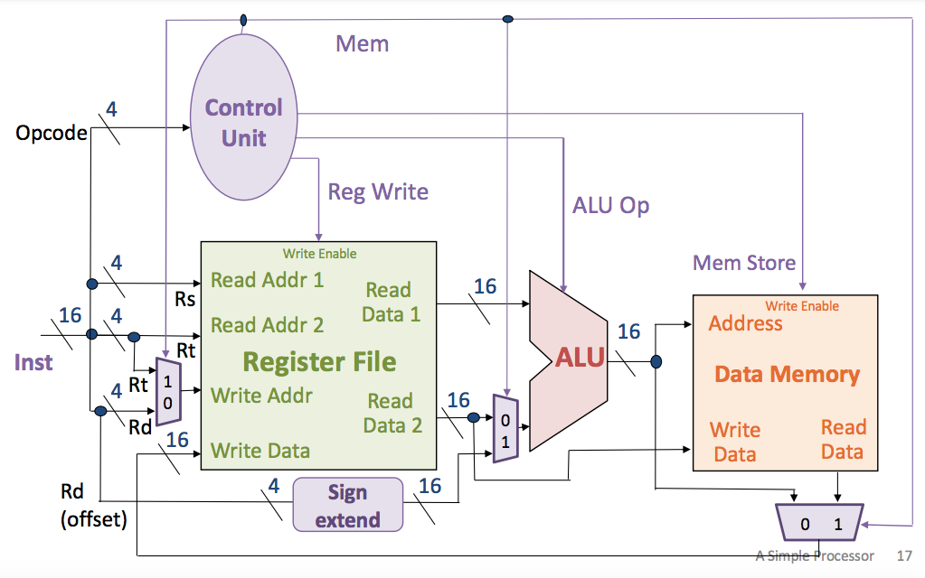
To distinguish between what is done in the dataptath for arithmetic/logic and control flow instructions (ADD, SUB, AND, OR, BEQ) versus what is done for memory access instructions (LW, SW), the following is necessary:
Use a 2x4 MUX at the input of the Register File to choose the source for the register to be written to (Rd gets written to for arithmetic/logic operations, Rt gets written to for LW).
Use a 2x16 MUX at the second input to the ALU. The MUX selects whether the ALU input comes from Rt or from the offset specified by the third operand of the instruction.
| Instruction | Datapath Action |
|---|---|
| ADD Rs Rt Rd | ALU performs Rs + Rt and stores result in Rd |
| SW Rs Rt offset | ALU performs Rs +
offset and sends result as Address to
Data Memory. Then value in Rt is stored to *Data Memory at specified address. |
| LW Rs Rt offset | ALU performs Rs +
offset and sends result as Address to
Data Memory. Then value at specified address in Data Memory is loaded to Rt. |
Exercise 8:
Below we have specified several operations by giving the relevant instruction values Rs, Rt, and Rd/offset as well as the Control Unit output values derived from the Opcode part of an instruction.
Refer to the table from the previous part about which ALU Op specifies which ALU function.
Before predicting the following operations, assume that all registers contain a value of 0 initially except R1 (which contains a 1). But assume that the registers are NOT reset between operations.
For each operation, predict the ALU result (in decimal) and explain which registers or memory locations would get a new value as a result of the operation.
Operation 1:
| ALUop | Rs | Rt | Rd/offset | RegWrite | Mem | MemStore | ALU result |
|---|---|---|---|---|---|---|---|
| 2 | 1 | 1 | 6 | 1 | 0 | 0 | Correct answer: 2 |
Explain the operation and result, and what register is modified with what new value:
Example answer: Addition of R1 with itself. R1 + R1 = 1 + 1, stored in R6. R6 gets a 2.
Operation 2:
| ALUop | Rs | Rt | Rd/offset | RegWrite | Mem | MemStore | ALU result |
|---|---|---|---|---|---|---|---|
| 2 | 6 | 6 | 3 | 1 | 0 | 0 | Correct answer: 4 |
Explain the operation and result:
Example answer: Addition of R6 with itself. R6 + R6 = 2 + 2, stored in R3. R3 gets a 4.
Operation 3:
| ALUop | Rs | Rt | Rd/offset | RegWrite | Mem | MemStore | ALU result |
|---|---|---|---|---|---|---|---|
| 2 | 6 | 1 | 6 | 0 | 1 | 1 | Correct answer: 8 |
Assume that Operation 3 is a Store Word (SW) instruction. Explain how you would know this from the values of the control signals.
Example answer: Mem being 1 means it’s either LW or SW. MemStore being 1 means it’s SW.
What value would be stored to what address in Data Memory?
The value stored is from Rt, which is a 1, so the contents of register 1 are being copied into memory. That register always has the value 1.
The address to store to is given by the value of register Rs plus the offset specified where Rd would normally be given. So in this case, that’s Rs = R6, with value 2, plus offset = 6 gives us address 8.
Operation 4:
| ALUop | Rs | Rt | Rd/offset | RegWrite | Mem | MemStore | ALU result |
|---|---|---|---|---|---|---|---|
| 2 | 3 | 6 | 4 | 1 | 1 | 0 | Correct answer: 8 |
Assume that Operation 4 is a Load Word (LW) instruction. Explain how you would know this from the values of the control signals.
Example answer: Mem being 1 means it’s either LW or SW. MemStore being 0 means it’s LW.
What address in Data Memory is being accessed?
Example answer: The address being accessed is address 8, the same one we just wrote to. But the way it’s computed is different. This time Rs = R3, and the offset is 4, so we compute 4 + 4 = 8.
What register will receive what new value from that address in Data Memory?
Example answer: R6 gets the value 1, which was previously stored in address 8.
Stretch Exercises: Control Unit
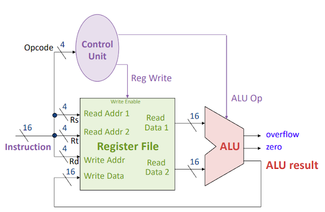
You have seen that the ALU Op bits (which control the operation of the ALU) are not the same as the instruction opcode (which specifies which instruction is being executed).
It is necessary to translate the instruction opcode to the proper ALU operation (which specifies ainv bneg op1 op0 into the ALU) for each instruction, as shown below:
| Instruction | opcode | ALU operation | ALU operation encoding | ||||||
| O3 | O2 | O1 | O0 | ainv | bneg | op1 | op0 | ||
| LW | 0 | 0 | 0 | 0 | ADD | 0 | 0 | 1 | 0 |
| SW | 0 | 0 | 0 | 1 | ADD | 0 | 0 | 1 | 0 |
| ADD | 0 | 0 | 1 | 0 | ADD | 0 | 0 | 1 | 0 |
| SUB | 0 | 0 | 1 | 1 | SUB | 0 | 1 | 1 | 0 |
| AND | 0 | 1 | 0 | 0 | AND | 0 | 0 | 0 | 0 |
| OR | 0 | 1 | 0 | 1 | OR | 0 | 0 | 0 | 1 |
| BEQ | 0 | 1 | 1 | 1 | SUB | 0 | 1 | 1 | 0 |
Note: The JMP instruction is not shown in this table because it does not use the ALU.
Exercise 9:
Explain why LW and SW have the same ALU operation as ADD:
Example answer: Because they need to add the address register to the offset that comes as part of the opcode to get the actual address to read from or write to.
Write a Boolean function for each ALU operation bit in terms of the opcode “O0-O3” inputs.
ainv = 0 (always off in these examples)
bneg = Example answer: O1O0
op1 = Example answer: O2’ + O2O1O0 (could be simplified to O2’ + O1)
op0 = Example answer: O2O1’O0
The logic to produce the ALU Op bits (which you just designed) is part of the Control Unit.
The Control Unit also produces the other data path control signals for each instruction, as shown below:
| Instruction | opcode | Reg Write | Mem | Mem Store | Branch | Jump | | | ||||
| O3 | O2 | O1 | O0 | ||||||
| LW | 0 | 0 | 0 | 0 | 1 | 1 | 0 | 0 | 0 |
| SW | 0 | 0 | 0 | 1 | 0 | 1 | 1 | 0 | 0 |
| ADD | 0 | 0 | 1 | 0 | 1 | 0 | 0 | 0 | 0 |
| SUB | 0 | 0 | 1 | 1 | 1 | 0 | 0 | 0 | 0 |
| AND | 0 | 1 | 0 | 0 | 1 | 0 | 0 | 0 | 0 |
| OR | 0 | 1 | 0 | 1 | 1 | 0 | 0 | 0 | 0 |
| BEQ | 0 | 1 | 1 | 1 | 0 | 0 | 0 | 1 | 0 |
| JMP | 1 | 0 | 0 | 0 | 0 | 0 | 0 | 0 | 1 |
Explain why the Reg Write bit is set for LW, ADD, SUB, AND, OR, but not for SW, BEQ, or JMP:
Example answer: The operations where RegWrite is set are operations where a result is written to a register. SW, BEQ, and JMP don’t write to a register: SW writes to memory instead, and BEQ and JMP change the PC.
Write a boolean function for each control line as a function of the opcode bits O0-O3:
RegWrite = Example answer: (O3’O2’O1’O0 + O2O1O0 + O3)’
Mem = Example answer: O3’O2’O1’
Mem Store = Example answer: O3’O2’O1’O0
Branch = Example answer: O2O1O0
Jump = Example answer: O3
Although we will not do so in lab today, you can see that it is easy to implement the Control Unit with basic logic gates.
Extra Exercises: Full Implementation
Download the computer.cct circuit and open it in LogicWorks.
Close the timing window and parts palette in LogicWorks to view the full circuit:
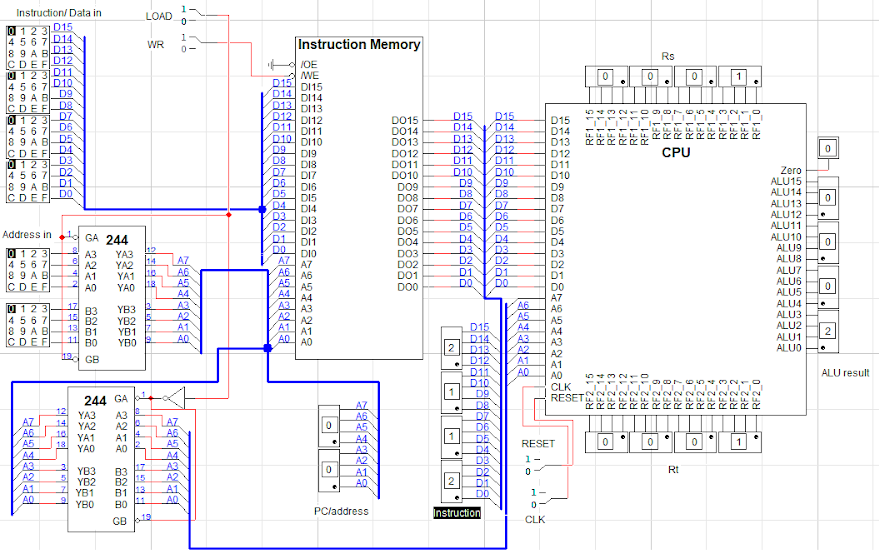
The CPU has been abstracted to a black box, and is connected to the Instruction Memory, where programs must be loaded prior to execution by the CPU.
The WR, LOAD, Instruction/Data in, and Address in inputs on the left are used to load a program into Instruction Memory.
LOAD is used to control the 244 devices that you see on the bottom left, and is needed for proper operation of the circuit for loading a program vs. running a program (the 244 is a multi-input/output tri-state buffer that can be set to let data through or appear disconnected; the LOAD switch toggles whether the top or bottom buffer is activated). Simply follow the instructions given later for how to use it.
The PC/address and Instruction hex displays on the bottom show the address in Instruction Memory currently being executed, and the instruction itself.
The Rs and Rt register file ports and the ALU result from the CPU are also displayed. These can be used to verify correct execution of instructions.
The Reset and CLK switches on the bottom are used to control execution of a program in the CPU. The following program will perform a loop (the first three instructions initialize registers to values to be used in the calculation).
Exercise 10:
Fill in the hexadecimal value for each encoded instruction in the table below, including values to make the BEQ and JMP instructions reach the intended lines:
| Address | Instruction | op | Rs, Rt, Rd/offset | Purpose |
|---|---|---|---|---|
| 0: | 2112 | ADD | R1, R1, R2 | ; R2 = 2 |
| 2: | Correct answer: 2223 | ADD | R2, R2, R3 | ; R3 = 4 |
| 4: | Correct answer: 2334 | ADD | R3, R3, R4 | ; R4 = 8 |
| 6: (LOOP) | Correct answer: 3424 | SUB | R4, R2, R4 | ; R4 <- R4 - R2 |
| 8: | Correct answer: 4444 | AND | R4, R4, R4 | ; display the result of the subtraction |
| A: | Correct answer: 7422 | BEQ | R4 R2 NEXT | ; escape the loop when R4 = 2 |
| C: | Correct answer: 8003 | JMP | LOOP | ; repeat the loop |
| … | ||||
| 10: (NEXT) | Correct answer: 1032 | SW | R0, R3, 2 | ; store 4 at address 2 in data memory |
| 12: | Correct answer: 1244 | SW | R2, R4, 4 | ; store 2 at address 6 in data memory |
| 14: | Correct answer: 0052 | LW | R0, R5, 2 | ; load 4 from address 2 in memory into R5 |
| 16: | Correct answer: 4555 | AND | R5, R5, R5 | ; display the contents of R5 = 4 |
| 18: | Correct answer: 5555 | OR | R5, R5, R5 | ; will also display 4 |
To load the Instruction Memory with this program:
- Set LOAD = 0
- Set address and data switches for one instruction
- Set WR = 0, then back to 1
Repeat until all instructions are loaded to memory.
To execute the program:
- Set LOAD = 1
- Set Reset = 1, then back to 0
- Set CLK = 1, then back to 0, for each instruction. Stop the first time PC = 8, and examine the output of the ALU. The first time, you should see the value of 6 displayed at the ALU output.
Keep executing the program, examining the result each time PC = 8.
The program is finished when PC = 0x18. How many times was the loop repeated? Correct answer: 3
Write a Program
Exercise 11:
Assume that after the previous exercise, you have a value of 4 stored in address 2 and a value of 2 stored in address 6 in Data Memory.
Write a program which will add those two values together, and store the result in address 8 in Data Memory. Write your program as a series of hexadecimal instructions in the table below, using registers 5 and 6 to store the data after loading it from memory, and register 7 to hold the addition result before loading it back into memory:
| Address | Instruction (hexadecimal) | Explanation |
|---|---|---|
| 0 | 0052 | Example answer: Load from address 2 into R5 |
| 2 | Correct answer: 0066 | Example answer: Load from address 6 into R6 |
| 4 | Correct answer: 2567 | Example answer: Add R5 + R6 and store in R7 |
| 6 | Correct answer: 1078 | Example answer: Store R7 in memory address 8 |
Load your program into the Instruction Memory and verify that it works correctly.
Now, write a program which will load from memory addresses 2 and 6 and multiply those two values using a loop with successive addition (use the R2 and R3 registers to hold the loaded values, and R4 for the result. Record your program below:
| Address | Instruction (hexadecimal) | Explanation |
|---|---|---|
| 0 | 0022 | Example answer: Load from address 2 into R2 |
| 2 | Correct answer: 0036 | Example answer: Load from address 6 into R3 |
| 4 | Correct answer: 5004 | Example answer: Zero out R4 |
| 6 | Correct answer: 2244 | Example answer: Add R2 and R4, overwriting R4 |
| 8 | Correct answer: 3313 | Example answer: Subtract 1 from R3, updating it |
| A | Correct answer: 7301 | Example answer: Skip the following JMP if R3 is 0 |
| C | Correct answer: 8003 | Example answer: Jump back to address 6, to add again |
Note that at the end, you can use instruction 4444 to show register 4 which should hold the result.
Load your program into the Instruction Memory and verify that it works correctly.