
🔬 Lab
CS 240 Lab 1
Basic Electronics and Digital Logic
CS 240 Lab 1
Basic Electronics and Digital Logic
In your first CS 240 lab, you will begin your study of computer systems by building physical circuits to experiment with basic electronics. You will be introduced to the protoboard and tools used to build circuits, and you will investigate the operation of a transistor, and how it can be used to implement circuits that produce simple logic functions.
You will also begin to learn about digital logic, experimenting with Boolean functions and basic gates.
Warm-up Questions
Based on the preparatory videos you watched, you should understand some basic concepts about electricity. Refer to the following circuit diagram:

Try to answer the questions below, using the “check my answer” and “show instructor answer” buttons to check your answers.
If we remove the resistor from the circuit and replace it with a wire, what would happen?
Example answer: This would create a “short circuit” which would quickly drain the battery, while causing the wire to heat up. Basically, as much current as possible will quickly flow through the wire, and something will fail (ideally, the battery’s charge; less ideally, the wire will heat up from residual resistance and melt through before the battery dies).
What if we remove the resistor, but leave the wire ends disconnected?
Example answer: This would create an “open circuit” where no current can flow, so nothing happens.
Calculate the current in the circuit using Ohm’s Law, using the indicated voltage and resistance values. Include the unit symbol for current in your answer, with an appropriate metric prefix so that the answer is an integer: Correct answer: 5 mA Feedback: Ohm’s Law is , where is current. Feedback: The symbol for amperes is ‘A’, so your answer must end with that. Explanation: Ohm’s law is , so to compute current (‘I’) we divide voltage by resistance. In this case, that’s 5 volts divided by 1000 ohms, which works out to 0.005 A, or alternatively, 5 mA.
If the resistor had a larger resistance value (assuming the voltage was the same) would there be more or less current?
more
less
Explanation: Ohm’s law states , so solving for current ‘I’ we get . This means that as resistance increases, the denominator gets bigger so the final result goes down. This makes sense because ‘resistance’ resists current.If the voltage source had a larger value (with the same resistance) would there be more or less current?
more
less
Explanation: Using the same math as the previous explanation, since voltage is in the numerator of the current equation, more voltage = more current. Intuitively, higher voltage = worse shock.
Your First Circuit
To practice the basics of using the prototyping station, you’ll cut and strip a new wire, and use it to power an logic indicator on the protoboard.
This picture shows the workbenches we’ll be using for digital logic prototyping (this is the older model; some of you have a newer model, but it has all the same pieces just with fancier logic indicators):
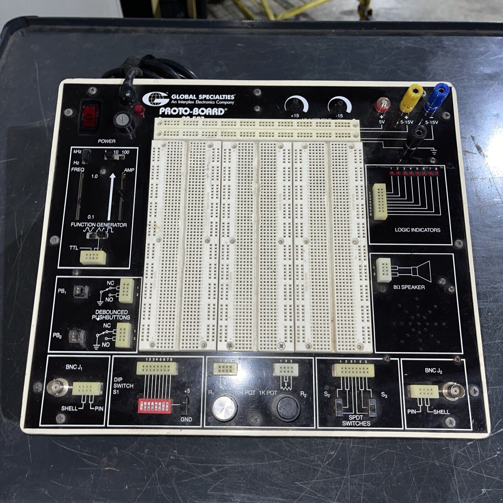
Refer to these slides to review the different parts of the workbench.
You should have a bag of wires on your table, along with a pair of wire cutters or strippers. Follow these steps:
Turn off your workbench.
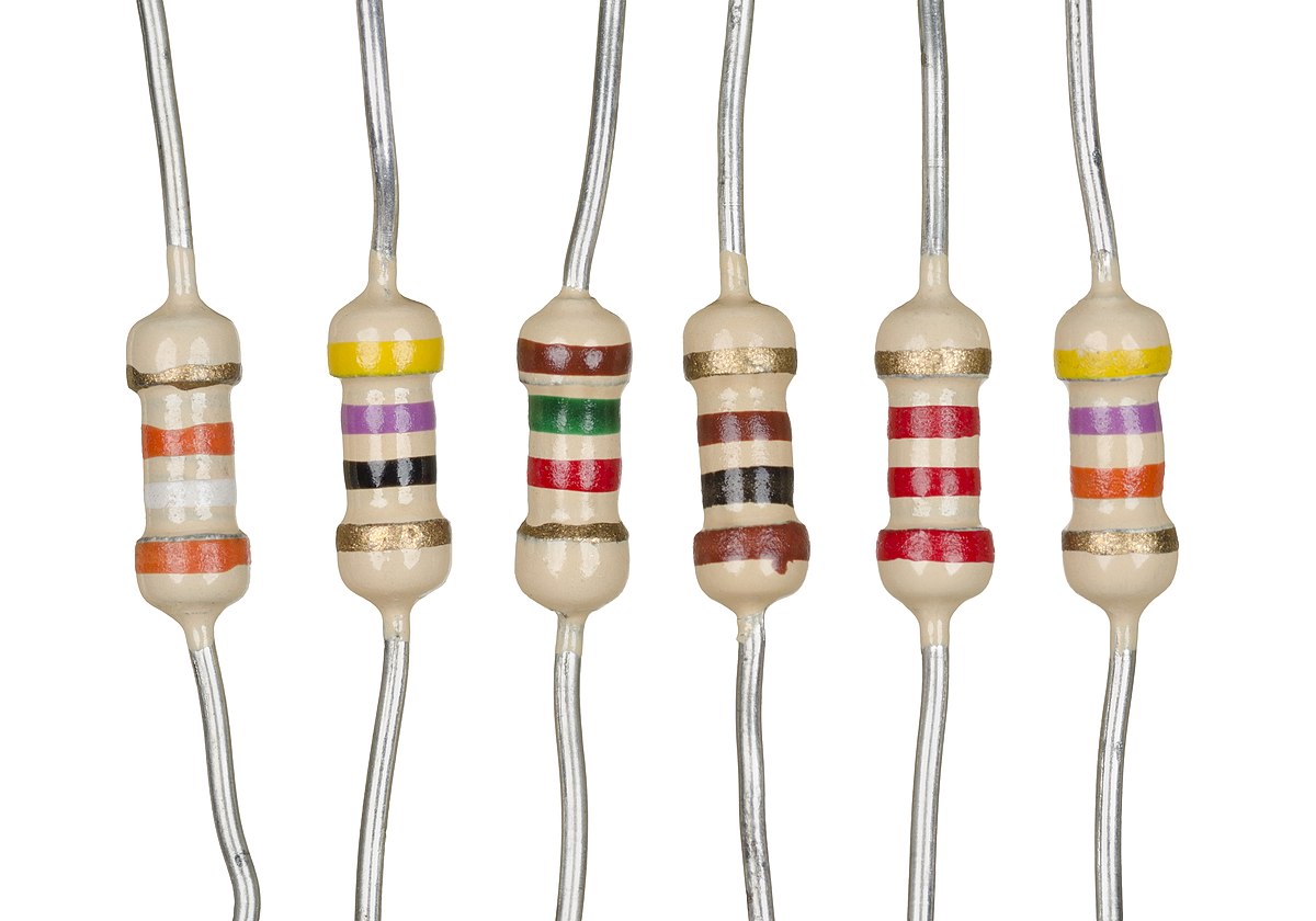
Ask for a spool of wire and a resistor, or retrieve one of each from the blue supply cabinet. Resistors look like this:
Measure a length that’s sufficient to reach from the top middle of the protoboard area over to the upper-right side where the logic indicators are.
Cut the wire, and then cut off the last ~1/2 centimeter of the plastic wrapper, either carefully using wire cutters or using a wire stripper if you have one (in that case you can put the wire into one of the holes and clamp down, then pull sideways). Let your partner try this step as well. Use the wires in your bag of wires as a reference.
Plug one end of your newly cut wire into a row of the protoboard near the middle, and the other end into one of the unused logic indicator input sockets. Make sure you plug into a row, and not into one of the side rails which are connected to power or ground.
Plug one leg of your resistor into the +5V rail near the row you plugged your wire into, and plug the other leg into the same row as your wire. This completes your circuit: power from the +5V terminal is delivered by the red jumper wires to the rail, then it can flow through the resistor to the row, through the row to the wire, through the wire to the logic indicator, and then through the indicator light (lighting it up in the process) out back to ground (the logic indicators are connected to ground inside the board).
Turn on the workbench. The logic indicator that you connected to should light up. If it doesn’t, ask for help.
Building Transistor Circuits
A transistor is a device that works like a switch - it can be turned on or off, Transistors are used to implement circuits that produce basic logic functions. In this exercise, you will experiment with a circuit which produces a simple logic function using a single 2N3904 transistor on the protoboard.
This interactive circuit simulator shows a circuit diagram that matches the circuit which should already be connected in the upper left corner of your prototyping board:
You can click on the ‘0’ at the left side next to the ‘A’ label and see the ‘1’ on the right side next to the ‘Q’ label change values. The two zig-zag sections are resistors, and the power is supplied at the top by the ‘+5V’ connection, while the wire connected to three descending parallel lines represents a connection to ground.
The component in the middle with two diagonal lines connecting to and from a larger vertical line represents a transistor. When voltage is available at the middle leg of the transistor, current from the top is able to flow down across the transistor to the ground connection. This prevents current from flowing to the ‘Q’ output, because the direct path downwards to ‘ground’ is shorter.
In contrast, when the voltage is toggled off at the middle input of the transistor, current can no longer flow through the transistor from top to bottom. In this way the transistor acts as an electrically-activated switch, either permitting current flow or blocking it. When flow is blocked, current from the voltage source at the top must flow out the ‘Q’ output to get to ground (we assume outputs will eventually be connected to ground), and so the voltage there will be high.
On your workbench, we connect the input ‘A’ through a push-button, so that when the button is pushed the voltage at ‘A’ will be high, and when it is not pushed it will be low. The output ‘Q’ is connected to an LED that will light up when current is available (or to a 2-LED logic indicator that lights up either a ‘low-voltage’ or ‘high-voltage’ LED).
Operate the circuit, both in real life and in the simulator, and confirm that they work the same. Record the output ‘Q’ for each possible input ‘A’ to produce a truth table for this circuit (click to cycle values):
GCorrect answer:
| A | Q |
|---|---|
| 0 | ? 0 1 |
| 1 | ? 0 1 |
Correct answer: See above
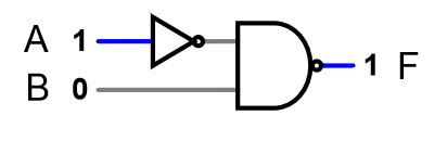
Describe the logic function produced by this circuit:
Example answer: It’s a NOT gate: high-voltage input results in low-voltage output, and vice versa.
Modify the circuit and connect the second transistor on your board to your current circuit, as shown in the circuit diagram below. Use the workbench’s second push-button as the input ‘B.’
Note: At intersections of two wires, a filled bubble indicates that there is actually a connection between the two wires at that point. Two wires which cross and do not use a filled bubble at the intersection are not physically connected.
Confirm that the simulator and physical circuit operate the same way, and fill in this truth table for the circuit:
GCorrect answer:
| A | B | Q |
|---|---|---|
| 0 | 0 | ? 0 1 |
| 0 | 1 | ? 0 1 |
| 1 | 0 | ? 0 1 |
| 1 | 1 | ? 0 1 |
Correct answer: See above
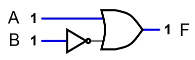
Describe the logic function produced by this circuit:
Example answer: The output is only high when both inputs are low. In other words, if A OR B is high, the output is low. Since an “OR” gate would be high under those circumstances, this is an inverted OR gate, also known as a NOR gate.
At this point, you should check in with the instructor to demonstrate that your circuit is working.
Circuit Diagrams
These tables show the Boolean Algebra notation, truth table, and circuit diagram symbol for the basic logic gates we’ll use in this class:
NOT
or
| A | F |
|---|---|
| 0 | 1 |
| 1 | 0 |

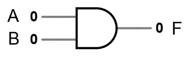
AND
| A | B | F |
|---|---|---|
| 0 | 0 | 0 |
| 0 | 1 | 0 |
| 1 | 0 | 0 |
| 1 | 1 | 1 |

OR
| A | B | F |
|---|---|---|
| 0 | 0 | 0 |
| 0 | 1 | 1 |
| 1 | 0 | 1 |
| 1 | 1 | 1 |

NAND
or
| A | B | F |
|---|---|---|
| 0 | 0 | 1 |
| 0 | 1 | 1 |
| 1 | 0 | 1 |
| 1 | 1 | 0 |

NOR
or
| A | B | F |
|---|---|---|
| 0 | 0 | 1 |
| 0 | 1 | 0 |
| 1 | 0 | 0 |
| 1 | 1 | 0 |

This simulator shows each basic gate and lets you try out inputs to see the resulting output:
Given the four circuits shown in this simulator:
Which of the circuit(s) shown are equivalent to the transistor circuit you built using two transistors in the previous part of the lab?
Circuit
1
Circuit
2
Circuit
3
Circuit
4
Explanation: The transistor
circuit from the previous part was a NOR gate, with formula
.
Circuit 1 is a NOT gate on one input of an AND gate, with formula
,
which is not equivalent. Circuit 2 is an OR gate with a NOT gate
afterwards, which is equivalent, and circuit 4 is just a NOR gate, which
is also equivalent. Circuit 3 is just an AND
gate.
Write a boolean function produced by the circuit shown in this simulator:
Note: It may be tempting to start by building a truth table for the circuit by manipulating the inputs in the simulator, but first try to analyze the circuit without interacting with it, and only use the simulator controls if you get stuck. You need to be able to understand circuits based on non-interactive diagrams.
Write your function here:
- Use apostrophe (and parentheses as needed) to indicate negation
- Use the 1-letter variable names ‘A’ and ‘B’
- Use Boolean algebra notation for AND and OR: AND just puts two letters next to each other; OR is written as a ‘+’.
- Don’t use any spaces or unnecessary parentheses in your answer.
F = Correct
answer: (A’B)’ Feedback: This answer is also correct, but the notebook
system can’t yet recognize multiple correct answers. I’m working on
that! Hint: Try to identify sub-components whose equivalent
gate you already know. Hint: You can also try to
think in terms of one input at a time. For example, in this circuit, if
‘A’ is 1, then ‘F’ will always be 1, regardless of ‘B’, so the formula
can be ‘A’ + something. Explanation: In this circuit,
the top-left transistor is hooked up to input ‘A’ in a configuration
that establishes the opposite of input ‘A’ on the top horizontal wire:
that top-left transistor is acting as a NOT gate. Then, the two
right-hand transistors act as two independent blockers, so that BOTH of
them must be open to let voltage drain out of the top where output ‘F’
is. This means that the top signal AND the bottom signal must both be
true to turn OFF the output F, which is a NAND gate. So the formula can
be written
.
An alternative analysis starts by recognizing that when ‘A’ is on, the
output is on no matter what B is doing, so the formula can be ‘A’ OR
something. When ‘A’ is off, the output F is just the negation of ‘B’,
because at that point the top transistor can let current through so the
bottom transistor acts as a NOT gate with ‘B’ as the input. So the full
formula will be
.
In fact, BOTH of these two formulae are correct and they are equivalent
to each other.
Now, on paper, draw a circuit diagram using basic gate symbols, leaving out the resistors. Don’t worry about trying to upload the result. You can leave this text box blank:
Example
answer: Here are two possible ways to draw
the circuit diagram, depending on the formula you chose:
 There are other correct drawings (for example the NAND gate in the first
drawing could instead be an AND gate feeding into a NOT gate).
There are other correct drawings (for example the NAND gate in the first
drawing could instead be an AND gate feeding into a NOT gate).
Building with Integrated Circuit Chips
Rather than building all of our logic out of transistors, it’s easier to think in terms of gates. Pre-packaged chips, called “integrated circuits,” “chips,” or “microchips,” contain internal transistor groups that implement basic gates (there are lots of other kinds of integrated circuits beyond these as well). ICs look like this:
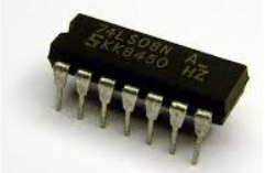
There are standardized chip designs that incorporate basic gates. The one shown above is a 7408 variant, specifically “74LS08N” which you can see printed on the top of the chip. (Sometimes the part number is very hard to read.) To understand the internal wiring of the chip, you need to look up the wiring diagram (also called a pinout because it shows which pins carry which signals out) for the chip. Thankfully, it’s still possible to find these by searching something like “7408 pinout” in most search engines. A data sheet usually includes a wiring diagram along with other specifications. Searching for the specific part number (e.g., “74LS08N pinout”) is generally safest. Here’s the diagram for the 7408 chip family:
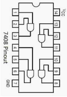
Note: Pretty much all ICs will include “Vcc” and “GND” pins, which must be connected to the +5V and ground wires on the workbench in order for the chip to function. In this diagram pin 14 is Vcc and ping 7 is GND.
Internally, this chip has 4 AND gates, accessible via pins 1-6 and 8-13. A 7408 chip is plugged into your board at the top right. Follow these steps to create the circuit shown below:
- Power off your board.
- Connect the Vcc pin of the 7408 to the +5V rail of the protoboard.
- Connect the GND pin of the 7408 to the ground rail of the protoboard.
- Look for the logic switches near the bottom left of the board. Connect a long-ish wire into one of the holes in the separate white plastic header for the switches, and stick the other end of that wire into the row that touches pin 1 of the 7408 (that’s the top-left-most pin).
- Connect a second logic switch output with pin 2 of the 7408.
- Connect pin 3 of the 7408 with one of the logic indicator sockets at the top right of your board. This will show the output of your circuit.
These connections can all be made with wires without worrying about adding resistors: the 7408 has a resistor internally to limit current flow from the voltage source, our inputs are all pre-wired with resistors, and the logic indicators on the board also have built-in resistors.
Once everything is connected, power the board on, and then flip the two switches you connected to see how they affect the output. Fill in the truth table below and check your answers to confirm it’s working correctly:
GCorrect answer:
| A | B | F |
|---|---|---|
| 0 | 0 | ? 0 1 |
| 0 | 1 | ? 0 1 |
| 1 | 0 | ? 0 1 |
| 1 | 1 | ? 0 1 |
Correct answer: See above
Bonus Task: A more complex circuit
Below the 7408 chip on the right side of your workbench, there should be a 7432 chip. Look up the pinout for that chip, and use it along with the 7408 to build the following circuit:
Verify that it works by filling in this truth table:
GCorrect answer:
| A | B | C | F |
|---|---|---|---|
| 0 | 0 | 0 | ? 0 1 |
| 0 | 0 | 1 | ? 0 1 |
| 0 | 1 | 0 | ? 0 1 |
| 0 | 1 | 1 | ? 0 1 |
| 1 | 0 | 0 | ? 0 1 |
| 1 | 0 | 1 | ? 0 1 |
| 1 | 1 | 0 | ? 0 1 |
| 1 | 1 | 1 | ? 0 1 |
Correct answer: See above
Write the Boolean Algebra formula for the circuit: - Don’t use parentheses or spaces.
F = Correct answer: AB+BC Explanation: The two AND gates accept A-and-B and B-and-C as inputs, and the results go to an OR gate, so the formula is an OR (‘+’) of two terms for ‘A and B’ and ‘B and C’. Parentheses are not needed since ‘multiplication’ = AND binds more tightly than ‘addition’ = OR.