Circuit Herbology
[Updated 17 Feb. to fix/clarify due dates and release Part II]
This full assignment is due Friday, 26 February and will be graded by Monday, 29 February, in advance of the exam on Tuesday, 1 March. You may OPTIONALLY submit one or both Parts in class Tuesday, 23 February – we will make every effort to grade this work earlier: hopefully by Friday, 26 February. You may submit your solutions all at once or submit the two Parts separately to take advantage of the early grading if you wish. There is no requirement to submit anything until the Friday, 26 February deadline.
ex Grow circuits and processor components.
- Checkpoint: if you want to use the OPTIONAL early grading, submit one or both Parts before class Tuesday, 23 February
- Due: before class Friday, 26 February
- Submit: Bring a paper copy to class.
- Relevant Reference:
- Collaboration: individual ex assignment policy, as defined by the syllabus.
Part I: Combinational Logic
1. Marauder’s Map
Draw a Karnaugh Map for the function F defined by the truth table below. Use the Karnaugh Map to derive a minimal sum-of-products Boolean formula for F. Show any intermediate work.
| A | B | C | D | F(A,B,C,D) |
| 0 | 0 | 0 | 0 | 1 |
| 0 | 0 | 0 | 1 | 1 |
| 0 | 0 | 1 | 0 | 1 |
| 0 | 0 | 1 | 1 | 0 |
| 0 | 1 | 0 | 0 | 0 |
| 0 | 1 | 0 | 1 | 1 |
| 0 | 1 | 1 | 0 | 0 |
| 0 | 1 | 1 | 1 | 1 |
| 1 | 0 | 0 | 0 | 1 |
| 1 | 0 | 0 | 1 | 0 |
| 1 | 0 | 1 | 0 | 1 |
| 1 | 0 | 1 | 1 | 0 |
| 1 | 1 | 0 | 0 | 0 |
| 1 | 1 | 0 | 1 | 1 |
| 1 | 1 | 1 | 0 | 0 |
| 1 | 1 | 1 | 1 | 1 |
2. Encoder
Draw a circuit to implement a 4-to-2 encoder using gates. An encoder is the opposite of a decoder. It takes 2n inputs and provides n outputs. Here, n = 2. Assume exactly one of the inputs carries a 1 and all others carry 0. The output should be an n-bit binary number giving the index of the input that is enabled. For example, if input 2 (in the range 0-3) is enabled and all others are disabled, the output should be 1 0.
3. Switching Network
Draw a circuit to implement a switching network with two data inputs (A and B), two data outputs (C and D), and a control input (S). If S is 1, the network is in pass-through mode: output C should equal input A and output D should equal input B. If S is 0, the network is in crossing mode: C should equal B, and D should equal A. Use whatever gates or combinational building blocks seem most reasonable.
4. Finishing the ALU
Background
In class, we showed how to design an n-bit ALU by connecting n 1-bit ALUs. Here is a 4-bit ALU based on our design:
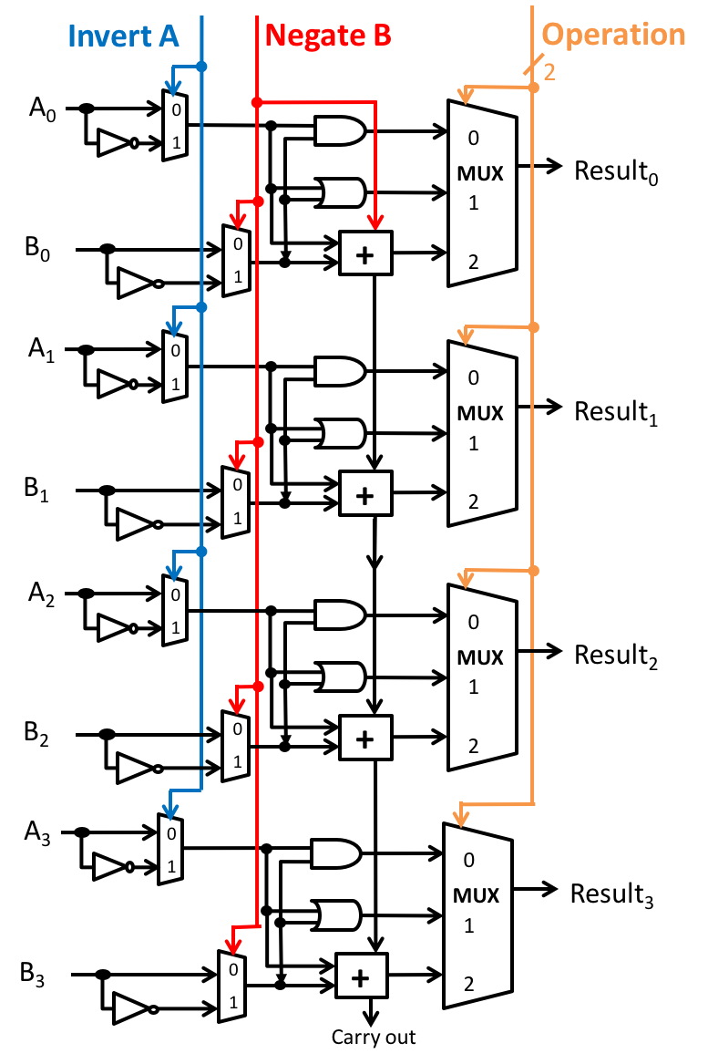
It is built from 1-bit ALUs of this form:
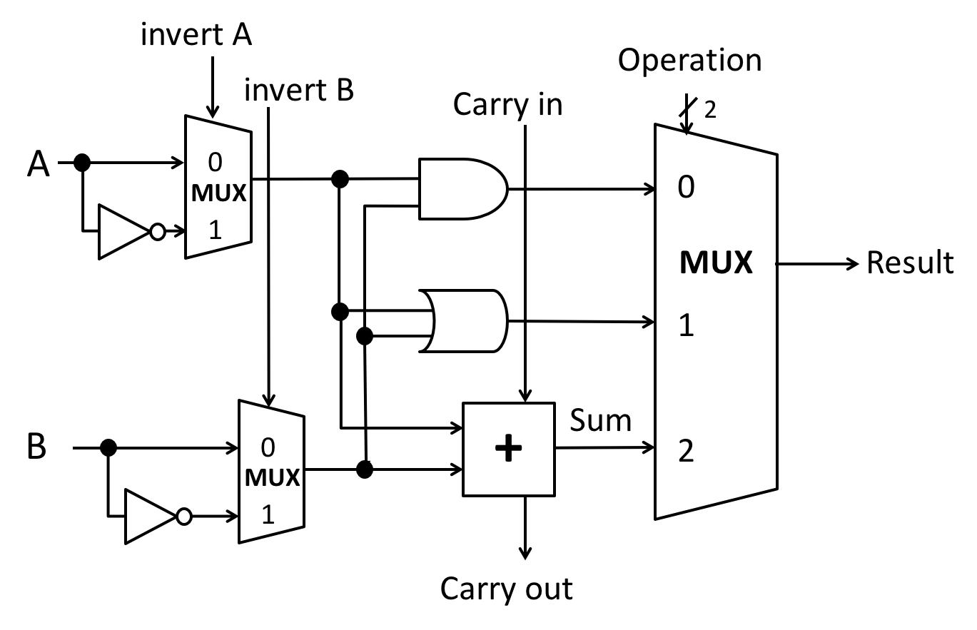
Recall that:
- The carry out from each bit is wired to the carry in of the next bit, if present.
- The full n-bit ALU has 4 lines of control input:
- invert A controls the invert A inputs of all of the 1-bit ALUs.
- negate B controls:
- the invert B inputs of all of the 1-bit ALUs; and
- the carry-in of the least significant bit ALU.
- Two bits of operation ID control the operation ID inputs of all of the 1-bit ALUs.
Guidelines
We considered adding several features to the ALU using minimal or no additional logic. However, some of our additions were incomplete. You will reimplement and improve these features in the exercises that follow.
- Use the same design, but consider a 4-bit ALU for simplicity.
- When asked to draw additional logic:
- Any additional circuitry may connect to any existing wires in the ALU and add gates or other building blocks as needed.
- Minimize the number of gates or other building blocks you add. Choose the simplest option.
- Use any gates (including arbitrarily large gates) or other building blocks we have discussed in class.
- Draw the additional logic required. Either:
- Draw it connecting to the ALU circuit diagram given above; or
- Label inputs to your added logic with text clearly describing where they connect to wires in the original ALU.
- Feel free to share logic among the different parts of the exercise.
- Write at most a short paragraph when asked for prose descriptions.
Exercises
-
Implement the four conditions codes (a) Zero Flag, (b) Sign Flag, (c) Carry Flag, and (d) Overflow Flag as extra 1-bit outputs from the n-bit ALU. You may find their definitions in the slides on ALUs. For each flag:
- Draw and label the additional logic required.
- Explain how your circuit works.
-
Describe the output of the ALU when Invert A = 1, Negate B = 1, and Operation ID = 10.
- Write your answer as an arithmetic or Boolean/bitwise expression using A and B, e.g., Result = A & B or Result = 2A / B.
- Your expression must use only arithmetic operators or only Boolean/bitwise operators. You may not mix them.
- Explain briefly how you derived your expression.
-
We discussed how to implement a less-than check for two’s-complement operands by computing A - B and inspecting the sign bit of the result.
- Describe why this approach seems to work at first glance. For example, consider checking if A < B for A = -310 =
1101and B = 210 =0010. - Consider A = -710 =
1001and B = 610 =0110. Unfortunately, our ALU will claim that -7 < 6 is false! Explain why. - Reimplement less-than so it works correctly for all pairs of 4-bit two’s-complement operands.
- Show the values to set on each of the 4 control lines of the full ALU.
- Draw any additional logic necessary to compute the correct less-than result as a 1-bit output of the full ALU, yielding 1 if the less-than property holds and 0 otherwise.
- Describe why this approach seems to work at first glance. For example, consider checking if A < B for A = -310 =
-
Implement an equality test output using minimal logic. Given inputs A and B, this output wire should carry 1 if A = B and 0 otherwise.
- Draw and label the additional logic required.
- Is your implementation susceptible to the same problem we encountered with less-than? Explain why or why not.
-
We implemented A NAND B and A NOR B using the existing ALU logic. Describe how to implement A XOR B. Do not add logic to the ALU, but do assume you have the capacity to save ALU results and reuse them later as inputs. You do not need to draw circuits or explain how to save and reuse results. Just describe your high-level approach to computing XOR briefly in English.
Part II: Memory and Microarchitecture
5. Flip-flopping
Consider the following circuits:
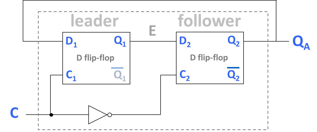
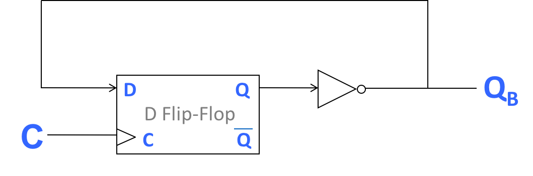
Note the similarity of the first circuit (A) to the implementation of a D flip-flop. We examined the second circuit (B) in class. All flip-flops used here follow the falling-edge trigger design used in lecture.
Explain the behaviors of QA and QB with respect to the clock C. Assume that QA and QB are both initially 0, E is intially 1, and both circuits are controlled by the same clock, C. Write no more than a short paragraph.
- Are the behaviors of QA and QB are related? (If so, are they identical?) Describe how and why their behaviors are or are not related.
- To support your claims, draw waveforms for C, QA, and QB. Show at least 4 full clock cycles, starting with C=0.
6. Memory Construction
In this group of exercises, you are given one or two AxB SRAMs, where A is the number of addresses or locations in the memory and B is the width of each location in bits. The provided SRAMS have the following form:
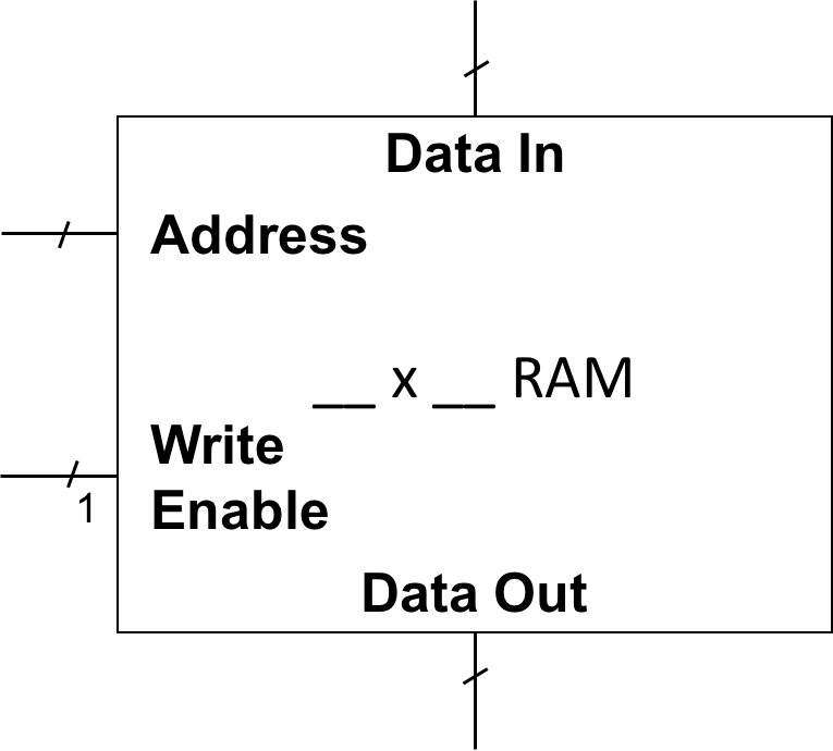
The SRAMs:
- have separate Data In and Data Out ports, plus an Address input and a Write Enable input;
- are always reading from the location given by the current Address, expressing its contents on Data Out;
- additionally store the value on Data In into the location given by the current Address, if the Write Enable input carries a 1; and
- are indivisible.
You will construct new SRAMs with the same kind of inputs, outputs, and externally observable behavior, but with different dimensions. For each, you will draw one or more small boxes of the form above (representing the provided SRAM) inside a larger box of the same form. You will connect inputs and outputs of the larger box with those of the smaller boxes, possibly adding combinational logic building blocks.
-
For a 256x4 SRAM, how wide (in bits/lines) is the Address input? Data In? Data Out? Each memory location?
In the next two exercises, do not draw each individual line in a bus (e.g., Address) unless necessary to distinguish the endpoints of the individual lines. Use hatch marks and width annotations instead.
- Construct a 256x8 SRAM by adding minimal logic to two identical 256×4 SRAM components.
-
Construct a 64K x 8 SRAM by adding minimal additional logic to a single provided 16K x 32 SRAM. (K = 1024)
- Unlike the previous exercise, the SRAM component provided in this exercise has the same capacity as the desired final product, though it has different dimensions:
- The addressable unit of data (i.e., the size of each memory location) is larger in the provided SRAM than in the SRAM you will build (32 bits vs. 8 bits).
- There are fewer memory locations in the provided SRAM than in the SRAM you will build (16K vs. 64K).
- Be careful with writes: when writing an 8-bit value into the provided SRAM, you must be sure not to destroy the other 24 bits that share the same underlying 32-bit cell.
- Unlike the previous exercise, the SRAM component provided in this exercise has the same capacity as the desired final product, though it has different dimensions:
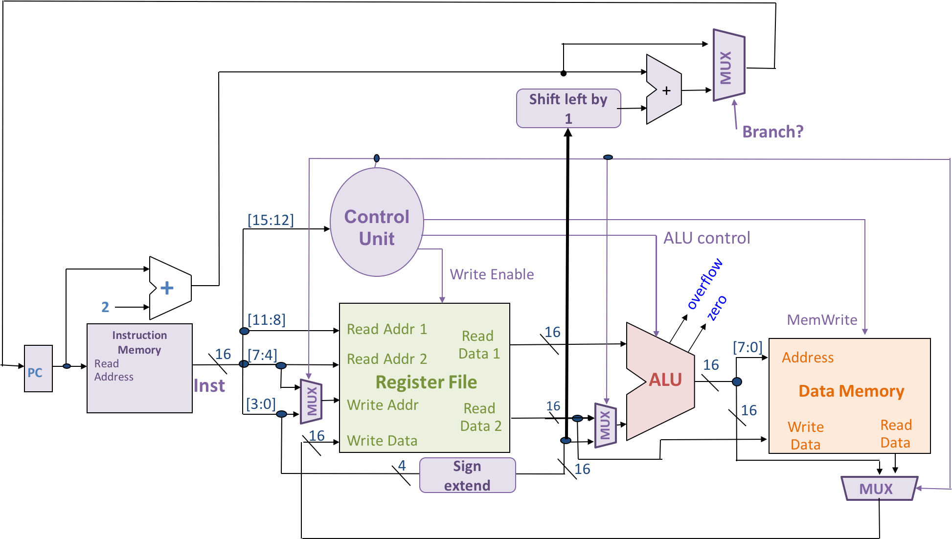
7. Shifting the Datapath
We wish to add an LSL (logical shift left) instruction to the toy architecture we developed in class. LSL Rs,Rt,Rd takes the value in register Rs, shifts it left logically by the number of bits given by the value in Rt, and stores the result value in register Rd. The LSL instruction will follow the encoding of arithmetic instructions, with the opcode 1001.
We will use the following shifter device to implement shifting. It takes a 16-bit data input and a 4-bit shift amount input, and produces a 16-bit output that is data input << shift amount.

- The data input and output are 16 bits to match the word size of our architecture. Why is the shift amount given in 4 bits?
- Connect the inputs and output of a Left Shifter in the toy processor datapath (shown below) to implement the LSL instruction. Use additional logic as needed. Refer to the class material for instruction encodings and other examples in our toy architecture.
- If connecting only a subset of lines from a bus, clearly mark which lines, using bit ranges as shown in the provided datapath diagram.
- Assume that the Control Unit already controls existing parts of the datapath properly for an LSL instruction given its opcode.
- Describe your design briefly (in at most a few sentences):
- How does your augmented datapath work to provide the shift instruction?
- Describe what the Control Unit must do differently for an LSL instruction vs. an AND instruction.
- If you added new control lines, describe how they should be controlled.