
Architecture
Assignment: Architecture
- Assign: Monday 12 February
- Due: Tuesday 20 February
- Policy: Individual graded synthesis assignment
- Submit: Upload a PDF written on the cs240-arch-worksheet-s24.pdf submission sheet
- Reference:
Goals
- To practice using combinational, arithmetic, and sequential logic.
- To understand how to encode computation with low-level building block including multiplexers, flip-flops, and adders.
- To master every piece of a simplified but representative instruction set architecture—the HW ISA.
Time reports
For a (slightly different) version of this assignment in a previous semester, students self-reported the following times:
- 25% of students spent <= 5 hours.
- 50% of students spent <= 7 hours.
- 75% of students spent <= 10 hours.
Contents
Exercises
Please write your answers on the cs240-arch-worksheet-s24.pdf submission sheet to streamline the grading process. Submit your work by scanning a PDF of all worksheet pages (in order) and uploading it to Gradescope. Remember that this course uses your Gradescope account attached to your Wellesley email address (the variety that matches your username). You can merge accounts across multiple email addresses if helpful.
Notes:
- This assignment is worth 75 points.
Q1. vALUe Judgments [22 points]
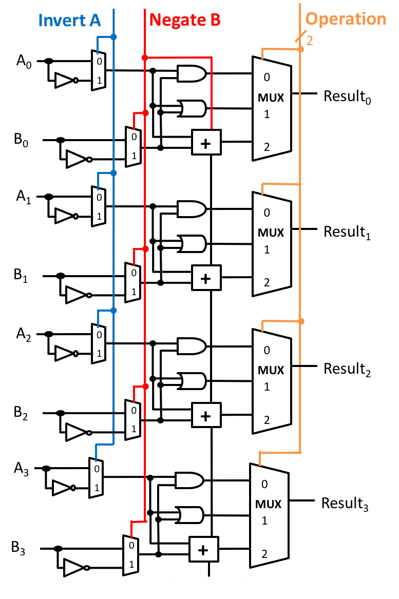
In class and lab we designed an $n$-bit ALU by connecting $n$ 1-bit ALUs. In these exercises, you will improve the 4-bit version of our design.
Summary of our ALU design:
- The
Carry outfrom each bit is wired to theCarry inof the next bit, if present. - The full $n$-bit ALU has 4 lines of control input:
Invert Acontrols theinvert Ainputs of all of the 1-bit ALUs.Negate Bcontrols:- the
invert Binputs of all of the 1-bit ALUs; and - the carry-in of the least-significant bit ALU.
- the
- Two bits of
Operation IDcontrol theOperationinputs of all of the 1-bit ALUs.

Rules for extending the ALU:
- Any additional logic may connect to any existing wires in the ALU and add gates or other building blocks as needed.
- Minimize the number of gates or other building blocks you add. Gates such as
ANDcan have > 2 inputs. - Choose the simplest option and clearly label new outputs.
Exercises:
-
[5 points] Design extra 1-bit outputs from the $n$-bit ALU for the four conditions codes. Using the provided sheet, draw and label the additional logic required for each condition code (flag), all on one ALU diagram.
Zero Flag:1if all bits of the result are0, otherwise0.Sign Flag:1if the result is negative, otherwise0.Carry Flag:1if there is a carry out from the operation, otherwise0.Overflow Flag:1if there is a signed overflow, otherwise0.
-
[12 points] Alice is trying to design a
Less-Thanflag output that computes $A < B$ for the 4-bit two’s-complement values $A$ and $B$. Her first idea is to compute $A - B$ and return a value based on the sign bit of the result: her hope is that a 0 sign bit for the result of the subtraction means $A \geq B$ and a 1 sign bit for the result means $A < B$.- [3 points]
Give three pairs of values, $A$ and $B$, where Alice’s approach
correctly calculates $A < B$.
- In the first pair, both $A$ and $B$ should be positive numbers.
- In the second pair, both $A$ and $B$ should be negative numbers.
- In the third pair, one of the two numbers should be positive and one should be negative.
- Note: Recall that 4-bit two’s complement values range from [-8, 7].
- [2 point] Give two pairs of values, $A$ and $B$, where Alice’s approach is incorrect in calculating
$A < B$ (that is, where her approach either yields 0 when $A$ actually is less than $B$, or 1 when $A$ is not actually less than $B$).
- In the first pair, $A$ should be positive.
- In the second pair, $A$ should be negative.
- [1 point] Describe the key effect that causes Alice’s approach’s answer from the previous part to be incorrect.
- [5 points] Using minimal additional logic, help Alice design a 1-bit
Less-ThanFlag whose value always correctly indicates $A < B$ after $A - B$ is performed. That is, the newLess-Thanflag should have value 1 if $A < B$ and 0 otherwise.- Using the provided sheet, draw and label your design.
- [1 point] Write how to control each of the 4 control lines of our 4-bit ALU to perform $A < B$:
Invert A = ?Negate B = ?Operation = ??
- [3 points]
Give three pairs of values, $A$ and $B$, where Alice’s approach
correctly calculates $A < B$.
-
[5 points] Design a 1-bit
EqualityFlag output for the ALU using minimal additional logic (but no additional XOR gates). Given inputs $A$ and $B$, this output wire should carry 1 if $A == B$ and 0 otherwise.- [4 points] Using the provided sheet, draw and label your design.
- [1 point] Write how to control each of the 4 control lines of our 4-bit ALU
ALU to perform $A$ == $B$:
Invert A = ?Negate B = ?Operation = ??
Q2. Flop-flip-flopping [10 points]
Consider the following circuit that uses falling-edge triggered D flip-flops.
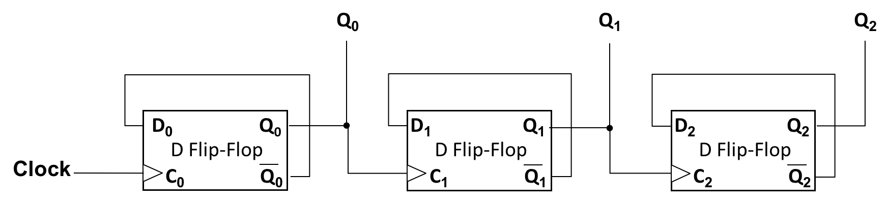
Assume the Clock input and values Q0, Q1, and Q2 are all initially 0. Draw waveforms for Clock, Q0, Q1, and Q2, showing at least ten Clock cycles. You do not need to turn in your waveform drawing, but it will help you reason about the circuit.
-
Fill in the table summarizing the values of Q0, Q1, and Q2 after each Clock cycle. Note the order that the worksheet table lists Q0, Q1, and Q2: this will help you identify a pattern in the next part.
-
Briefly explain what this circuit does at a high level, treating the Q outputs as a single multi-bit value. A phrase to a couple sentences is enough. Hint: you have seen a similar circuit behavior in lab.
Q3. Some Loopy Programs [19 points]
In this exercise you will simulate the execution of more HW ISA programs with loops.
Background
As an example, we consider a different program that has a loop to remind
you of the conventions used in an execution table (as
shown in the solution slides for the HW ISA architecture).
Suppose that register R2 has been initialized with
the signed decimal number 3 and register R3 has been initialized
with the signed decimal number 7. Also suppose that
the program P0 has the following Instruction Memory (IM):
IM
| Address | Contents |
| 0x0–0x1 | BEQ R2, R3, 3 |
| 0x2–0x3 | ADD R2, R1, R2 |
| 0x4–0x5 | SUB R3, R1, R3 |
| 0x6–0x7 | JMP 0 |
| 0x8–0x9 | HALT |
Then here is an execution table that shows the step-by-step execution of the
program P0.
Note that the way you should read the meaning of BEQ R1, R2, offset is
that the change to the PC, PC <- PC + 2 + offset*2 replaces the
non-branch change to the PC (PC <- PC + 2), as we designed in the
HW ARCH slides. Specifically, note in the following example that the PC
goes from 0 to 8 (not 10) based on the instruction BEQ R2, R3, 3, because
PC + 2 + offset*2 = 0 + 2 + 3*2 = 8.
Execution table
| PC | Instruction | State Changes |
| 0x0 | BEQ R2, R3, 3 | PC ← PC+2 = 0+2 = 2 (because 3 = R[2] != R[3] = 7) |
| 0x2 | ADD R2, R1, R2 | R[2] ← R[2]+R[1] = 3+1 = 4; PC ← PC+2 = 2+2 = 4 |
| 0x4 | SUB R3, R1, R3 | R[3] ← R[3]-R[1] = 7-1 = 6; PC ← PC+2 = 4+2 = 6 |
| 0x6 | JMP 0 | PC ← 2*0 = 0 |
| 0x0 | BEQ R2, R3, 3 | PC ← PC+2 = 0+2 = 2 (because 4 = R[2] != R[3] = 6) |
| 0x2 | ADD R2, R1, R2 | R[2] ← R[2]+R[1] = 4+1 = 5; PC ← PC+2 = 2+2 = 4 |
| 0x4 | SUB R3, R1, R3 | R[3] ← R[3]-R[1] = 6-1 = 5; PC ← PC+2 = 4+2 = 6 |
| 0x6 | JMP 0 | PC ← 2*0 = 0 |
| 0x0 | BEQ R2, R3, 3 | PC ← PC+2+(2*3) = 0+2+6 = 8 (because 5 = R[2] == R[3] = 5) |
| 0x8 | HALT | program stops executing |
Your Tasks
First, consider a HW ISA program P1 with the following Instruction Memory IM:
IM
| Address | Contents |
| 0x0–0x1 | ADD R0, R0, R2 |
| 0x2–0x3 | ADD R1, R1, R3 |
| 0x4–0x5 | ADD R3, R3, R4 |
| 0x6–0x7 | BEQ R3, R4, 3 |
| 0x8–0x9 | ADD R2, R4, R2 |
| 0xA–0xB | SUB R4, R1, R4 |
| 0xC–0xD | JMP 3 |
| 0xE–0xF | HALT |
-
[8 points] In the worksheet, fill in the execution table for program
P1. Use the same notational conventions used in the example execution table forP0above. Any numbers beginning with0xwill be interpreted as hexadecimal; any numbers not beginning with0xwill be interpreted as decimal. -
[3 points] Show the final values of the registers
R2,R3, andR4when the program execution halts. Again, any numbers beginning with0xwill be interpreted as hexadecimal; any numbers not beginning with0xwill be interpreted as decimal. -
[3 points] Alice wants to translate program
P1(except for the finalHALTinstruction) into a sequence of statements in a version of C with a 16-bitinttype. Fill in the rest of her program with assignments to variables namedR2,R3, andR4that represent the registers with these names inP1and awhileloop. You can use the online C compiler to check your C syntax.int R0 = 0; int R1 = 1; int R2 = R0 + R0; // ... -
[5 points] Consider this new loopy program,
P2, with the following instruction memory. AssumeR2andR3hold input values when the following program starts.R4will hold an output when the program stops. The address of each instruction in the instruction memory is shown at left. TheHALTinstruction stops the computer.# R2 and R3 hold program inputs here. 0x0: AND R2, R2, R4 0x2: AND R3, R3, R5 0x4: BEQ R5, R0, 3 0x6: SUB R5, R1, R5 0x8: ADD R4, R4, R4 0xA: JMP 2 0xC: HALT # Stops execution. # What value is in R4?- [3 points] Execute the program with the initial state that
R2holds4andR3holds3(you do not need to draw out the full execution table for this part). What are the final values in the registersR2,R3,R4, andR5when the program reachesHALT? You may write your answers in either decimal or hex, but must use a0xprefix for hex. - [2 points] Try a few more examples with (small) positive numbers in
R2andR3. What does this code do withR2andR3to computeR4? Answer with one simple line of valid C code of the form:R4 =exp;, where exp is a simple C expression using the the variablesR2andR3(corresponding to the HW registers) and any simple C operations that accomplish the same effect as these combined HW instructions. exp must not include C statements like loops or conditionals. It should also not include any function calls.
- [3 points] Execute the program with the initial state that
Q4. Taking Control [8 points]
In this exercise you will design the Control Unit for the HW microarchitecture we designed in class. (Base your design on the figure below labeled “HW microarchitecture datapath”.) Our design focused on connecting the datapath components (e.g., the register file, ALU, memory, etc.), but we left the Control Unit as black box.
Instead of drawing gates for the Control Unit, we will just build out a truth table for the behavior of the control unit. The truth table should take in a 4-bit HW instruction opcodes as input. As output, the truth table should produce control bits for each output control line, as needed for the specific opcode.
The worksheet provides the Control Unit table design. The control lines we need are:
- Reg Write (1 bit): controls the write-enable of the register file. If an instruction should both read and write to the register file, the write-enable should be 1 (that is, the read data lines still produce the contents of their respective registers even when the write-enable is 1).
- ALU Op (4 bits): controls the ALU (with the same 4 ALU control lines
we developed earlier; see the end of the Arithmetic slides).
- From left to right: Invert A, Negate B, Op1, Op0.
- Mem Store (1 bit): controls the write-enable of the data memory.
- Mem (1 bit): controls three multiplexers deciding which input to provide for:
- the register file’s write address; and
- the register file’s write data; and
- the ALU’s second operand.
- Branch (1 bit, added during class): controls whether to choose the next PC based on a branch target and test.
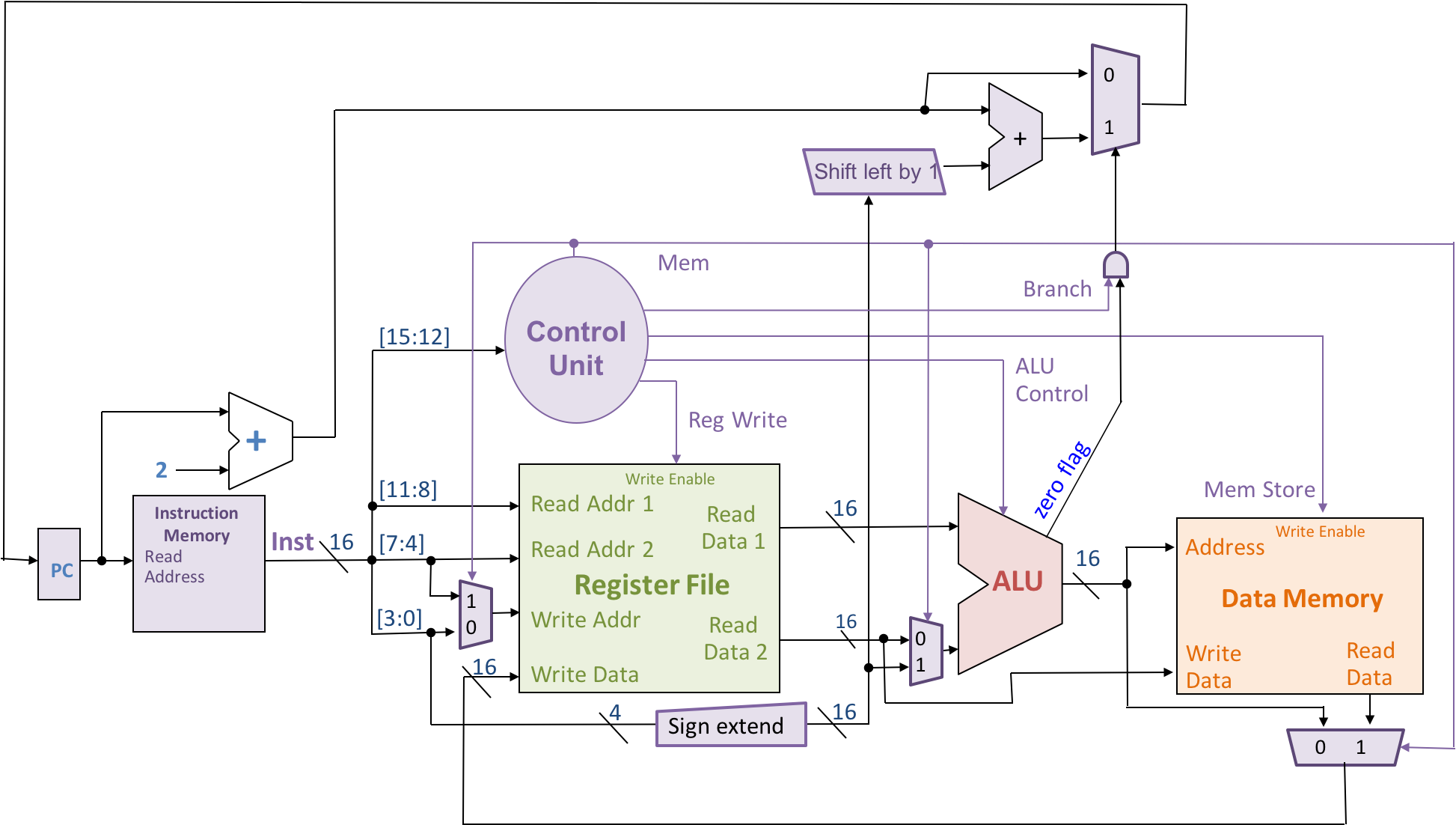
Your task for this problem is to fill in each of the row for each of the following instructions,
as shown on the worksheet: SW, ADD, SUB, AND, OR, BEQ.
For this problem, we will interpret all answers as binary (not decimal or hexadecimal).
We have completed the row for LW (“load”) as an example. For LW, the control lines are:
- Opcode:
0000, as shown in the HW ISA instruction table on slide 14, “HW ISA Instructions”, of the lecture slides - Reg Write:
1, since loads do write to the register file - ALU Op:
0010, since for aLW, the design needs to add the offset to a register’s contents. - Mem Store:
0, since loads do not write to the memory. - Mem:
1, to control the 3 multiplexers for the register file’s write and the ALU’s second operand. - Branch:
0, since the design should not branch for the load instruction (LWshould use the standard increment-PC-by-2 calculation).
Q5. Instruction NOT Missing (8 points)
The HW ISA introduced in class lacks an instruction for bitwise
not. A logical choice would be NOT Rs,Rd, which takes the
bitwise not of the value in source register Rs and stores
into destination register Rd. While we could implement NOT with a
sequence of existing HW ISA instructions (doing so would be a good practice
exercise to test your understanding!), in this problem, we will add
a new direct encoding for NOT to the HW ISA.
- [3 points] We will first implement a related instruction,
NAND, as a new ISA instruction. In the worksheet, fill in a 16-bit encoding of theNANDinstruction, following the format shown in the instruction table on slide 14, “HW ISA Instructions”, of the lecture slides. Choose any unused opcode for the encoding. -
[3 points] Fill in the labeled row of the Control Unit Table from earlier in the worksheet, to indicate how to control the datapath to implement
NAND. Do not add extra logic to the datapath diagram—instead, use properties of boolean operations to calculateNANDusing the logic already present. - [2 points] Consider how to implement
NOTusingNAND. Define an encoding for theNOTinstruction directly in the ISA. Choose the encoding carefully to minimize additions to the Control Unit and the datapath. Assuming you have completed the previous parts of this problem, the encoding should requires no new rows or columns in the Control Unit table.
Q6. Jumping into the Unknown [8 points]
Add logic to the HW microarchitecture depicted in the figure above to implement the
JMP instruction, which we did not implement in class. JMP sets the PC to the absolute instruction address
given by its argument (a number) multiplied by 2. For example,
JMP 3 sets the PC to 0x6, causing the instruction stored at
address 0x6 (i.e., the 3rd instruction in the program) to be
executed next.
-
[6 points] In the wiring diagram for the microarchitecture on the worksheet, you will add:
-
One new Jump control line from the Control Unit (in Problem 4), carrying 1 if the current instruction is
JMPand 0 otherwise. -
Wiring and logic using the Jump control line and the offset bits from the
JMPinstruction encoding to store theJMPinstructions’s target address to the PC if and only if the current instruction isJMP. Be sure to label any ranges of bits when splitting a wire (as done in the diagram for other operands).
Notes:
-
The
JMPhardware will need to use a Zero Extend unit that is different from the existing Sign Extend unit. -
Do not attempt to reuse the existing Shift unit; if you need such a shift, use a separate copy.
-
-
[1 point] In the Control Unit truth table from earlier in the worksheet, flesh out the contents of the the Jump control line in the final column.
-
[1 points] In the Control Unit truth table from earlier in the worksheet, flesh out the contents of the row for the
JMPopcode.
Submission
Please write your answers on the cs240-arch-worksheet-s24.pdf submission sheet to streamline the grading process. Submit your work by scanning a PDF of all worksheet pages (in order) and uploading it to Gradescope. Remember that this course uses your Gradescope account attached to your Wellesley email address (the variety that matches your username). You can merge accounts across multiple email addresses if helpful.